Can ship immediately
Due to market price fluctuations,if you need to purchase or consult the price.You can contact us or emial to us: brenda@hongda-ic.com
1. Describe
The 74LVT16245BDGGRG4 device is a 16-bit (dual octal) non-inverting tri-state transceiver designed for low-voltage (3.3V) VCC operation, but can provide a TTL interface for a 5V system environment. These devices are designed for asynchronous communication between two data buses. Logic level Direction control (DIR) input and output enable (OE) input to activate port B output or port A Output or put both output ports in high impedance mode. The device transmits data from the A bus to When the B port output is activated, the B bus is activated, and the A port output is activated from the B bus to the A bus positive. The input circuits on the A and B ports are always active and must have a logic high or low level to prevent excessive ICC and ICCZ. When VCC is between 0 and 1.5 V, the device is in a high-impedance state when it is powered on or off. However, in order to ensure a high impedance state above 1.5V, OE needs to be connected to VCC through a pull-up resistor; the minimum value of the resistor is determined by the current sink capability of the driver. These devices are perfectly suitable for me Three-state shutdown and power-up. I close the circuit Disable the output to prevent damage to the current backflow through the device in the event of a power failure. The power-on tri-state circuit puts the output in a high impedance state during power-up and power-off, This prevents driver conflicts.
2. Feature
1. Member of Texas Instruments Widebus™ series
2. The most advanced advanced BiCMOS technology (ABT) design that can achieve 3.3V operation and low static power consumption
3. Support mixed mode signal operation (5V input and output voltage with 3.3V VCC)
4. Supports unregulated battery operation as low as 2.7 V
5. Typical VOLP (output ground bounce) <0.8 V, VCC = 3.3 V, TA = 25°C
6. Ioff and Power-Up 3 states support hot plugging
7. Distributed VCC and GND pins minimize high-speed switching noise
8. Circulation architecture optimizes PCB layout
9. Latch up performance exceeds 100 mA, in line with JESD 78, Class II
10. ESD protection exceeds JESD 22
– 2000-V Human Body Model (A114-A)
– 200-V machine model (A115-A)
– 1000V charging equipment model (C101)
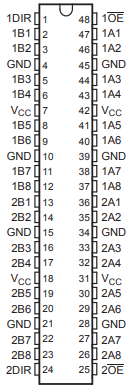
3. Pin configuration

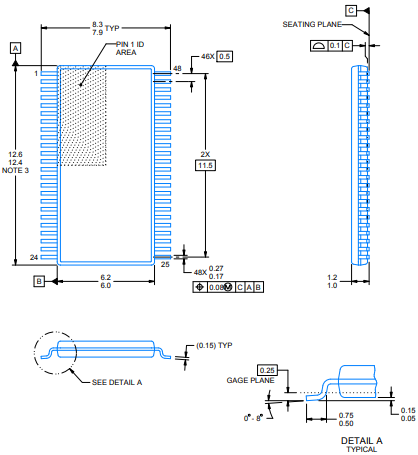
4. Package overview
