Can ship immediately
Due to market price fluctuations,if you need to purchase or consult the price.You can contact us or emial to us: brenda@hongda-ic.com
1. GENERAL DESCRIPTION
The AD7533KR is a low cost, 10-bit, 4-quadrant multiplying DAC manufactured using an advanced thin-film-on-monolithicCMOS wafer fabrication process. Pin and function equivalent to the AD7533KR industry standard, the AD7533KR is recommended as a lower cost alternative for old AD7533KR sockets or new 10-bit DAC designs. AD7533KR application flexibility is demonstrated by its ability to interface to TTL or CMOS, operate on 5 V to 15 V power, and provide proper binary scaling for reference inputs of either positive or negative polarity.
2. FEATURES
1. Low cost 10-bit DAC
2. Low cost AD7520 replacement
3. Linearity: ½ LSB, 1 LSB, or 2 LSB
4. Low power dissipation
5. Full 4-quadrant multiplying DAC
6. CMOS/TTL direct interface
7. Latch free (protection Schottky not required)
8. Endpoint linearity
3. APPLICATIONS
1. Digitally controlled attenuators
2. Programmable gain amplifiers
3. Function generation
4. Linear automatic gain controls
4. GENERAL CIRCUIT INFORMATION
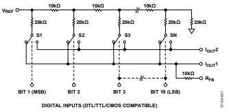
The AD7533KR is a 10-bit multiplying DAC that consists of a highly stable thin-film R-2R ladder and ten CMOS current switches on a monolithic chip. Most applications require the addition of only an output operational amplifier and a voltage or current reference. The simplified D/A circuit is shown in Figure 7. An inverted R- 2R ladder structure is used, that is, the binarily weighted currents are switched between the IOUT1 and IOUT2 bus lines, thus maintaining a constant current in each ladder leg independent of the switch state.

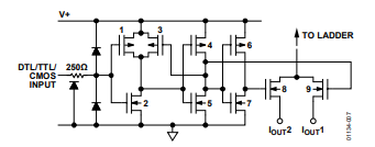
One of the CMOS current switches is shown in . The geometries of Device 1, Device 2, and Device 3 are optimized to make the digital control inputs DTL/TTL/CMOS compatible over the full military temperature range. The input stage drives two inverters (Device 4, Device 5, Device 6, and Device 7), which in turn drive the two output N channels. The on resistances of the switches are binarily sealed so that the voltage drop across each switch is the same. For example, Switch 1 in designed for an on resistance of 20 Ω, Switch 2 for 40 Ω, and so on. For a 10 V reference input, the current through Switch 1 is 0.5 mA, the current through Switch 2 is 0.25 mA, and so on, thus maintaining a constant 10 mV drop across each switch. It is essential that each switch voltage drop be equal if the binarily weighted current division property of the ladder is to be maintained.
