Can ship immediately
Due to market price fluctuations,if you need to purchase or consult the price.You can contact us or emial to us: brenda@hongda-ic.com
1. Description
The AMC1100DUB is a precision isolation amplifier with an output separated from the input circuitry by a silicon dioxide barrier that is highly resistant to magnetic interference. This barrier is certified to provide galvanic isolation of up to 4250 VPEAK, according to DIN VDE V 0884-11: 2017-01 and UL1577. Used in conjunction with isolated power supplies, this device prevents noise currents on a high common-mode voltage line from entering the local ground and interfering with or damaging sensitive circuitry. The AMC1100 input is optimized for direct connection to shunt resistors or other low voltage level signal sources. The excellent performance of the device enables accurate current and voltage measurement in energy-metering applications. The output signal common-mode voltage is automatically adjusted to either the 3-V or 5-V low-side supply. The AMC1100 is fully specified over the extended industrial temperature range of –40°C to +105°C and is available in the SMD-type, wide-body SOIC-8 (DWV) and gullwing-8 (DUB) packages.
2. Features
1. ±250-mV input voltage range optimized for shunt resistors
2. Very low nonlinearity: 0.075% max at 5 V
3. Low offset error: 1.5 mV max
4. Low noise: 3.1 mVRMS typ
5. Low high-side supply current: 8 mA max at 5 V
6. Input bandwidth: 60 kHz min
7. Fixed gain: 8 (0.5% Accuracy)
8. High common-mode rejection ratio: 108 dB
9. Low-side operation: 3.3 V
10. Safety-related certifications:
– 4250-VPK basic isolation per DIN VDE V 0884-11: 2017-01
– 3005-VRMS isolation for 1 minute per UL1577
– CAN/CSA no. 5A-component acceptance service notice and DIN EN 61010-1 standard
– Working voltage: 1200 VPEAK
– Transient immunity: 2.5 kV/µs min
11. Fully specified over the extended industrial temperature range
3. Applications
1. Electricity meters
2. String inverters
3. Power measurement applications
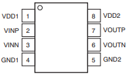
4. Pin configuration

5. Pin Description

6. Function description
The differential analog input of the AMC1100 is a switched capacitor circuit based on a second order modulator Stage that digitizes an input signal into a 1-bit output stream. The device compares differential input signals Charge and discharge at a typical frequency of 10 MHz using a continuous internal capacitor relative to the 2.5 V internal reference. With the S1 switch closed, CIND charges to the voltage difference between VINP and VINN. For the discharge phase, the two S1 switches are opened first, and then the S2 switch is closed. During this phase, CIND discharges to approximately GND1 + 0.8 V. The analog input range is tailored to directly accommodate the voltage drop across the shunt resistor for current sensing. However, the analog input signal has two limitations, VINP and VINN. If the input voltage is out of range GND1 – 0.5 V to VDD1 + 0.5 V, the input current must be limited to 10 mA to protect Implemented input protection diodes from damage. In addition, the linearity and noise performance of the device Guaranteed only if the differential analog input voltage remains within ±250 mV.