Can ship immediately
Due to market price fluctuations,if you need to purchase or consult the price.You can contact us or emial to us: brenda@hongda-ic.com
1. Describe
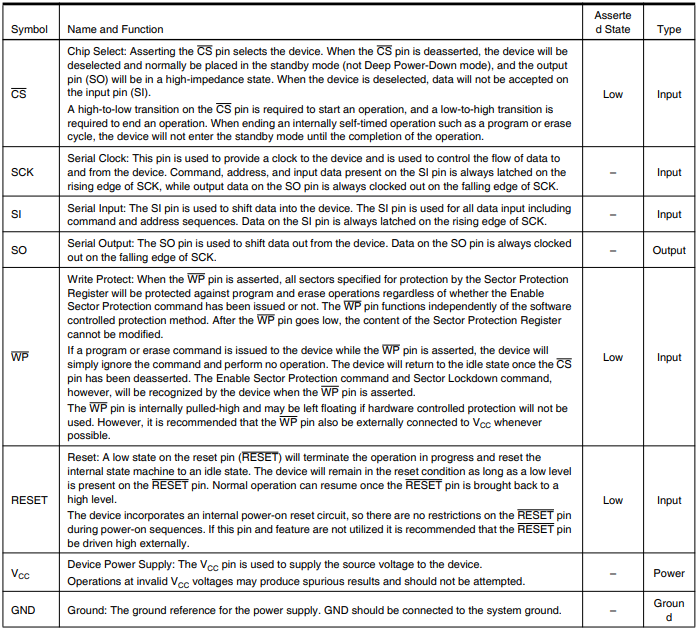
AT45DB021D-SH-T is a 2.7V serial interface flash memory, very suitable for various digital voice, image, program code and data storage applications. AT45DB021D supports RapidS™ serial interface, suitable for applications that require very high-speed operation. The RapidS serial interface is compatible with SPI, and the frequency is up to 66MHz. Its 2-,162-,688-bit memory is organized into 1,024 pages, each with 256 bytes or 264 bytes. In addition to the main memory, AT45DB021D also contains a 256/264 byte SRAM buffer. EEPROM emulation (bit or byte variability) can be easily handled through independent three-step read-modify-write operations. Unlike traditional flash memory that uses multiple address lines and a parallel interface for random access, DataFlash® uses the RapidS serial interface to access its data sequentially. Simple sequential access significantly reduces the number of effective pins, promotes hardware layout, improves system reliability, minimizes switching noise, and reduces package size. The device is optimized for many commercial and industrial applications that require high density, low pin count, low voltage, and low power consumption. In order to achieve simple in-system reprogramming, AT45DB021D does not require high input voltage for programming. The device uses a single power supply ranging from 2.7V to 3.6V for programming and reading operations. AT45DB021D is enabled through the chip select pin (CS) and accessed through a three-wire interface consisting of serial input (SI), serial output (SO) and serial clock (SCK). All program and erase cycles are self-timed.
2. Feature
1. 2.7V to 3.6V single power supply
2. RapidS serial interface: 66MHz maximum clock frequency
– SPI compatibility mode 0 and 3
3. User configurable page size
– 256 bytes per page
– 264 bytes per page
– The page size can be pre-configured at the factory to 256 bytes
4. Page programming operation
– Intelligent programming operation
– 1,024 pages (256/264 bytes/page) main memory
5. Flexible erasing options
– Page erase (256 bytes)
– Block erase (2 KB)
– Sector erase (32 KB)
– Chip Erase (2-Mbits)
6. 1 SRAM data buffer (256/264 bytes)
7. Continuous read capability of the entire array
– Ideal for code shadow applications
8. Low power consumption
– 7mA active reading current typical
– 25μA typical standby current
– 15μA deep power-down (typical value)
9. Hardware and software data protection function
– Individual departments
10. Department lock for security code and data storage
– Individual departments
11. Security: 128-byte security register
– 64 bytes of user programmable space
– Unique 64-byte device identifier
12. JEDEC standard manufacturer and device ID read
13. At least 100,000 program/erase cycles per page
14. Data retention-20 years
15. Industrial temperature range
16. Green (lead-free/halide-free/RoHS compliant) package options
3. Pin configuration
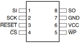
4. Pin description