Can ship immediately
1. Detailed Description
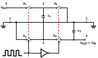
The ICL7660S and ICL7660A contain all the necessary circuitry to complete a negative voltage converter, with the exception of two external capacitors, which may be inexpensive 10µF polarized electrolytic types. The mode of operation of the device may best be understood by considering Figure 1, which shows an idealized negative voltage converter. Capacitor C1 is charged to a voltage, V+,for the half cycle, when switches S1 and S3 are closed.
(Note: Switches S2 and S4 are open during this half cycle).
During the second half cycle of operation, switches S2 and S4 are closed, with S1 and S3 open, thereby shifting capacitor C1 to C2 such that the voltage on C2 is exactly V+, assuming ideal switches and no load on C2. The ICL7660S and ICL7660A approach this ideal situation more closely than existing non-mechanical circuits.

FIGURE 1. IDEALIZED NEGATIVE VOLTAGE CONVERTER
In the ICL7660S and ICL7660A, the four switches of Figure 1 are MOS power switches; S1 is a P-Channel device; and S2, S3 and S4 are N-Channel devices. The main difficulty with this approach is that in integrating the switches,the substrates of S3 and S4 must always remain reverse biased with respect to their sources, but not so much as to degrade their “ON” resistances. In addition, at circuit startup, and under output short circuit conditions (VOUT = V+),the output voltage must be sensed and the substrate bias adjusted accordingly. Failure to accomplish this would result in high power losses and probable device latch-up.
This problem is eliminated in the ICL7660S and ICL7660A by a logic network that senses the output voltage (VOUT) together with the level translators, and switches the substrates of S3 and S4 to the correct level to maintain
necessary reverse bias.
The voltage regulator portion of the ICL7660S integral part of the anti-latchup circuitry; however, its inherent voltage drop can degrade operation at low voltages. Therefore, to improve low voltage operation, the “LV” pin should be connected to GND, thus disabling the regulator. For supply voltages greater than 3.5V, the LV terminal must be left open to ensure latchup-proof operation and to prevent device damage
2. What to do and what not to do
1. Do not exceed the maximum power supply voltage.
2. Do not connect the LV terminal to GND to obtain the power supply voltage Greater than 3.5V.
3. Do not short-circuit the output to V+ power supply for power supply Long-term voltage higher than 5.5V; however,Transient conditions including startup are acceptable.
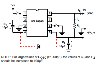
4. When using polarized capacitors, the + terminal of C1 must Connect to pin 2 of ICL7660S, and The + terminal of C2 must be connected to GND.
5. If the voltage drive ICL7660S has a large source impedance (25Ω to 30Ω), then A 2.2µF capacitor from pin 8 to ground may be required Limit the rate of rise of the input voltage to less than 2V / µs.
6. If the input voltage is higher than 5V and has a rising rate Over 2V/µs, external Schottky diode from VOUT CAP- is required to prevent latch-up (by By keeping the output forward biased the body diode of Q4) (Pin 5) is more active than CAP- (Pin 4).
7. The user should ensure that the output (pin 5) is not conducting More positive than GND (pin 3). The device latch will Occurs under these conditions. Provide additional Protection, placing 1N914 or similar diodes in parallel Using C2 can prevent the device from Under these conditions, when the load on VOUT creates a path Pull up VOUT before the IC is active (anode pin 5,Cathode needle 3)
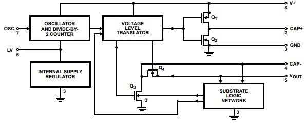
3. Functional Block Diagram

4. ICL7660S TEST CIRCUIT
