Can ship immediately
Due to market price fluctuations,if you need to purchase or consult the price.You can contact us or emial to us: brenda@hongda-ic.com
1. Description
The LM2673SX-ADJ/NOPB series of regulators are monolithic integrated circuits which provide all of the active functions for a step-down (buck) switching regulator capable of driving up to 3-A loads with excellent line and load regulation characteristics. High efficiency (>90%) is obtained through the use of a low ONresistance DMOS power switch. The series consists of fixed output voltages of 3.3 V, 5 V, and 12 V and an adjustable output version. The SIMPLE SWITCHER® concept provides for a complete design using a minimum number of external components. A high fixed frequency oscillator (260 kHz) allows the use of physically smaller sized components. A family of standard inductors for use with the LM2673 are available from several manufacturers to greatly simplify the design process. Other features include the ability to reduce the input surge current at power on by adding a soft-start timing capacitor to gradually turn on the regulator. The LM2673 series also has built-in thermal shutdown and resistor programmable current limit of the power MOSFET switch to protect the device and load circuitry under fault conditions. The output voltage is ensured to a ±2% tolerance. The clock frequency is controlled to within a ±11% tolerance.
2. Features
1. Efficiency Up to 94%
2. Simple and Easy to Design With (Using Off-TheShelf External Components)
3. Resistor Programmable Peak Current Limit Over a Range of 2 A to 5 A
4. 150-mΩ DMOS Output Switch
5. 3.3-V, 5-V, 12-V Fixed Output and Adjustable (1.2 V to 37 V) Versions
6. ±2% Maximum Output Tolerance Over Full Line and Load Conditions
7. Wide Input Voltage Range: 8 V to 40 V
8. 260-KHz Fixed Frequency Internal Oscillator
9. Soft-Start Capability
10. –40 to 125°C Operating Junction Temperature Range
3. Applications
1. Simple-to-Design, High Efficiency (>90%) StepDown Switching Regulators
2. Efficient System Preregulator for Linear Voltage Regulators
3. Battery Chargers
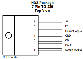
4. Pin Configuration

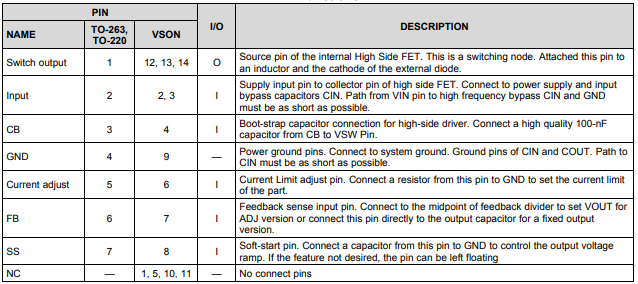
5. Pin Functions

6. Switch Output
This is the output of a power MOSFET switch connected directly to the input voltage. The switch provides energy to an inductor, an output capacitor and the load circuitry under control of an internal pulse-width-modulator (PWM). The PWM controller is internally clocked by a fixed 260-kHz oscillator. In a standard step-down application the duty cycle (Time ON/Time OFF) of the power switch is proportional to the ratio of the power supply output voltage to the input voltage. The voltage on pin 1 switches between VIN (switch ON) and below ground by the voltage drop of the external Schottky diode (switch OFF).
7. Input
The input voltage for the power supply is connected to pin 2. In addition to providing energy to the load the input voltage also provides bias for the internal circuitry of the LM2673. For ensured performance the input voltage must be in the range of 8 V to 40 V. For best performance of the power supply the input pin must always be bypassed with an input capacitor located close to pin 2.
8. C Boost
A capacitor must be connected from pin 3 to the switch output, pin 1. This capacitor boosts the gate drive to the internal MOSFET above VIN to fully turn it ON. This minimizes conduction losses in the power switch to maintain high efficiency. The recommended value for C Boost is 0.01 µF.
9. Ground
This is the ground reference connection for all components in the power supply. In fast-switching, high-current applications such as those implemented with the LM2673, TI recommends that a broad ground plane be used to minimize signal coupling throughout the circuit.
10. Current Adjust
A key feature of the LM2673 is the ability to tailor the peak switch current limit to a level required by a particular application. This alleviates the need to use external components that must be physically sized to accommodate current levels (under shorted output conditions for example) that may be much higher than the normal circuit operating current requirements. A resistor connected from pin 5 to ground establishes a current (I(pin 5) = 1.2 V / RADJ) that sets the peak current through the power switch. The maximum switch current is fixed at a level of 37,125 / RADJ.
11. Feedback
This is the input to a two-stage high gain amplifier, which drives the PWM controller. It is necessary to connect pin 6 to the actual output of the power supply to set the DC output voltage. For the fixed output devices (3.3-V, 5- V, and 12-V outputs), a direct wire connection to the output is all that is required as internal gain setting resistors are provided inside the LM2673. For the adjustable output version two external resistors are required to set the dc output voltage. For stable operation of the power supply it is important to prevent coupling of any inductor flux to the feedback input