Can ship immediately
Due to market price fluctuations,if you need to purchase or consult the price.You can contact us or emial to us: brenda@hongda-ic.com
1. Description
The LP5907MFX-3.3/NOPB is a low-noise LDO that can supply up to 250 mA output current. Designed to meet the requirements of RF and analog circuits, the LP5907 device provides low noise, high PSRR, low quiescent current, and low line or load transient response figures. Using new innovative design techniques, the LP5907 offers class-leading noise performance without a noise bypass capacitor and the ability for remote output capacitor placement. The device is designed to work with a 1-µF input and a 1-µF output ceramic capacitor (no separate noise bypass capacitor is required). This device is available with fixed output voltages from 1.2 V to 4.5 V in 25-mV steps. Contact Texas Instruments Sales for specific voltage option needs.
2. Features
1. Input voltage range: 2.2 V to 5.5 V
2. Output voltage range: 1.2 V to 4.5 V
3. Stable with 1-µF ceramic input and output capacitors
4. No noise bypass capacitor required
5. Remote output capacitor placement
6. Thermal-overload and short-circuit protection
7. –40°C to 125°C operating junction temperature
8. Low output voltage noise: < 6.5 µVRMS
9. PSRR: 82 dB at 1 kHz
10. Output voltage tolerance: ±2%
11. Very low IQ (enabled): 12 µA
12. Low dropout: 120 mV (typical)
13. Create a custom design using the LP5907 with the WEBENCH® Power Designer
3. Applications
1. Smartphones
2. Tablets
3. Communications equipment
4. Digital still cameras
5. Factory automation
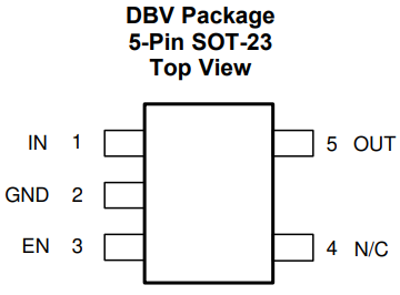
4. Pin Configuration
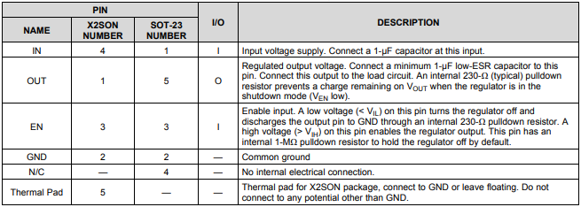
5. Pin Functions
6. Feature Description
1. Enable (EN)
The LP5907 EN pin is internally held low by a 1-MΩ resistor to GND. The EN pin voltage must be higher than the VIH threshold to ensure that the device is fully enabled under all operating conditions. The EN pin voltage must be lower than the VIL threshold to ensure that the device is fully disabled and the automatic output discharge is activated.
2. Low Output Noise
Any internal noise at the LP5907 reference voltage is reduced by a first order low-pass RC filter before it is passed to the output buffer stage. The low-pass RC filter has a –3 dB cut-off frequency of approximately 0.1 Hz.
3. Output Automatic Discharge
The LP5907 output employs an internal 230-Ω (typical) pulldown resistance to discharge the output when the EN pin is low, and the device is disabled.
4. Remote Output Capacitor Placement
The LP5907 requires at least a 1-µF capacitor at the OUT pin, but there are no strict requirements about the location of the capacitor in regards the OUT pin. In practical designs, the output capacitor may be located up to 10 cm away from the LDO.
5. Thermal Overload Protection (TSD)
Thermal shutdown disables the output when the junction temperature rises to approximately 160°C which allows the device to cool. When the junction temperature cools to approximately 145°C, the output circuitry enables. Based on power dissipation, thermal resistance, and ambient temperature, the thermal protection circuit may cycle on and off. This thermal cycling limits the dissipation of the regulator and protects it from damage as a result of overheating. The thermal shutdown circuitry of the LP5907 has been designed to protect against temporary thermal overload conditions. The TSD circuitry was not intended to replace proper heat-sinking. Continuously running the LP5907 device into thermal shutdown may degrade device reliability.
7. Application Information
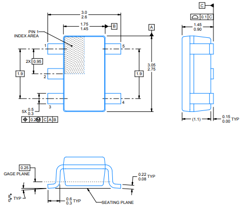
The LP5907 is designed to meet the requirements of RF and analog circuits, by providing low noise, high PSRR, low quiescent current, and low line or load transient response figures. The device offers excellent noise performance without the need for a noise bypass capacitor and is stable with input and output capacitors with a value of 1 µF. The LP5907 delivers this performance in industry standard packages such as DSBGA, X2SON, and SOT-23 which, for this device, are specified with an operating junction temperature (TJ ) of –40°C to 125°C.
8. Package overview