
Can ship immediately
Due to market price fluctuations,if you need to purchase or consult the price.You can contact us or emial to us: brenda@hongda-ic.com
1. Describe
The LT3582EUD-12#TRPBF are dual DC/DC converters With positive and negative outputs and integrated feedback Resistor. The LT3582 has built-in one-time programming (OTP) with configurable output settings via I2C interface, including output voltage settings, power-up sequencing, brownout discharge and output voltage slope. LT3582 The settings can be adaptively changed in the final product, or the settings in the manufacturing process and using the built-in permanent Non-volatile OTP memory. The positive output voltage can be Set between 3.2V and 12.775V in 25mV steps. negative Output Voltage Programmable Between –1.2V and –13.95V –50mV steps. LT3582-5 and LT3582-12 are preconfigured The ±5V and ±12V outputs are shipped from the factory, respectively, as This eliminates the need to use the I2C interface. The LT3582 family consists of two monolithic converters, One liter and one inverse. The boost converter has a Integrated power switch and output disconnect switch. Inverting Converter Using Single Inductor Topology and includes an integrated power switch. both boost and an inverting converter using a new precision control scheme resulting in low output voltage ripple while allowing high Conversion efficiency is over a wide range of load currents. this The LT3582 family is available in a 16-pin 3mm x 3mm QFN package.
2. Feature
1. Output voltage:
- 3.2V to 12.775V and –1.2V to –13.95V (LT3582)
- 5V and –5V (LT3582-5)
- 12V and –12V (LT3582-12)
2. Digitally reprogrammable via I2C (LT3582) for:
- The output voltage
- Power sequencing
- Output voltage ramp rate
3. Power-Up Defaults Programmable via Non-Volatile OTP (LT3582)
4. I2C compatible interface (standard mode*)
5. Integrated all power switches
- 350mA current limit (boost)
- 600mA current limit (inverting)
6. Integrated all feedback resistors
7. Input voltage range: 2.55V to 5.5V
8. Low quiescent current
- 325μA in active mode
- 0.01μA in shutdown mode
9. Integrated output disconnected
10. Tiny 16-pin 3mm × 3mm QFN package
3. Pin configuration
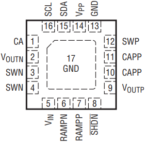
4. Application
1. AMOLED power supply
2. CCD power
3. Universal DC/DC conversion
5. Application Information
The LT3582 series are dual DC/DC converters, each containing a boost and an inverting converter. this Both boost and inverting converters use novel controls technique, which changes both peak inductances simultaneously Current and closing times. This leads to high efficiency over a wide load range and low output voltage ripple. exist In addition, the technology further reduces output ripple When the switching frequency is in the audio frequency band.
6. Boost converter
The boost converter uses ground A source NMOS power transistor acts as the main switching element. The current in the NMOS is constantly monitored and controlled, with the switch off time to achieve Regulation of VOUTP. VOUTP voltage divided by Internally Programmable (LT3582 Only) Resistor Divider Create FBP. The voltage on the FBP is compared to the internal voltage reference and zoom in, creating an error signal Control VCP node for proper peak inductance The current and off-time are for subsequent switching cycles.
7. Inverting Converter
Inverting converters use power PMOS transistor with source connected to VIN. this topology requires only an external inductor instead of Usually two inductors plus flying capacitors are required. Tuning is implemented in a similar way to Boost.

