Can ship immediately
1. Description
MC74LVX4066DR2G uses silicon gate CMOS technology Achieve fast propagation delay, low on-resistance and low Leakage current outside the channel. The bilateral switch/multiplexer/ Demultiplexer controls analog and digital voltages that may vary Across the entire power supply range (from VCC to GND). The pin arrangement of MC74LVX4066DR2G is the same as that of metal gate CMOS MC74LVX4066DR2G and high-speed CMOS HC4066A. Each device has four Independent switch. The design of the device makes The linearity of resistance (RON) in the input voltage range is much higher than that of RON Manufacturing of metal gate CMOS analog switches. On/off control input is compatible with standard CMOS Output; with pull-up resistors, they are compatible with LSTTL Output.
2. Features
1. Fast Switching and Propagation Speeds
2. High ON/OFF Output Voltage Ratio
3. Low Crosstalk Between Switches
4. Diode Protection on All Inputs/Outputs
5. Wide Power−Supply Voltage Range (VCC − GND) = 2.0 to 6.0 Volts
6. Analog Input Voltage Range (VCC − GND) = 2.0 to 6.0 Volts
7. Improved Linearity and Lower ON Resistance over Input Voltage than the MC14016 or MC14066
8. Low Noise
9. Chip Complexity: 44 FETs or 11 Equivalent Gates
10. These Devices are Pb−Free and are RoHS Compliant
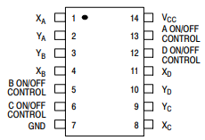
3. PIN CONNECTION

4. Application information
ON/OFF control pin should be in VCC or GND logic Level, VCC is recognized as a logic high level, and GND is recognized as a logic high level It is considered logically low. Unused analog input/output May be left floating (not connected). But this is It is recommended to connect unused analog inputs and outputs to VCC or GND passes through a low-value resistor. This minimizes crosstalk And unused feedthrough noise that may be picked up I/O pins. The maximum analog voltage swing depends on Power supply voltage VCC and GND. Positive peak simulation The voltage must not exceed VCC. Similarly, negative peaks The analog voltage should not be lower than GND. In this example Below, the difference between VCC and GND is 6 volts. Therefore, the maximum analog signal with a peak-to-peak value of six volts can be controlled. When the voltage transient is higher than VCC and/or lower than GND Expect to use an external diode (Dx) on the analog channel These diodes should be small signal, fast turn-on type that can absorb the signal The maximum expected current surge during clipping. One Another way is to replace the Dx diode with absorb.
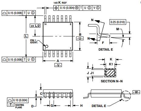
5. PACKAGE DIMENSIONS
