Can ship immediately
Due to market price fluctuations,if you need to purchase or consult the price.You can contact us or emial to us: brenda@hongda-ic.com
1. Description
DDR3 SDRAM uses a double data rate architecture to achieve high-speed operation. The double data rate architecture is an 8n-prefetch architecture with an interface designed to transfer two data words per clock cycle at the I/O pins. A single read or write operation for the DDR3 SDRAM effectively consists of a single 8n-bit-wide, four- clockcycle data transfer at the internal DRAM core and eight corresponding n-bit-wide, onehalf-clock-cycle data transfers at the I/O pins. The differential data strobe (DQS, DQS#) is transmitted externally, along with data, for use in data capture at the DDR3 SDRAM input receiver. DQS is center-aligned with data for WRITEs. The read data is transmitted by the DDR3 SDRAM and edge-aligned to the data strobes. The DDR3 SDRAM operates from a differential clock (CK and CK#). The crossing of CK going HIGH and CK# going LOW is referred to as the positive edge of CK. Control, command, and address signals are registered at every positive edge of CK. Input data is registered on the first rising edge of DQS after the WRITE preamble, and output data is referenced on the first rising edge of DQS after the READ preamble. Read and write accesses to the DDR3 SDRAM are burst-oriented. Accesses start at a selected location and continue for a programmed number of locations in a programmed sequence. Accesses begin with the registration of an ACTIVATE command, which is then followed by a READ or WRITE command. The address bits registered coincident with the ACTIVATE command are used to select the bank and row to be accessed. The address bits registered coincident with the READ or WRITE commands are used to select the bank and the starting column location for the burst access. The device uses a READ and WRITE BL8 and BC4. An auto precharge function may be enabled to provide a self-timed row precharge that is initiated at the end of the burst access. As with standard DDR SDRAM, the pipelined, multibank architecture of DDR3 SDRAM allows for concurrent operation, thereby providing high bandwidth by hiding row precharge and activation time. A self refresh mode is provided, along with a power-saving, power-down mode.
2. Features
1. VDD = VDDQ = 1.5V ±0.075V
2. 1.5V center-terminated push/pull I/O
3. Differential bidirectional data strobe
4. 8n-bit prefetch architecture
5. Differential clock inputs (CK, CK#)
6. 8 internal banks
7. Nominal and dynamic on-die termination (ODT) for data, strobe, and mask signals
8. Programmable CAS READ latency (CL)
9. Posted CAS additive latency (AL)
10. Programmable CAS WRITE latency (CWL) based on tCK
11. Fixed burst length (BL) of 8 and burst chop (BC) of 4 (via the mode register set [MRS])
12. Selectable BC4 or BL8 on-the-fly (OTF)
13. Self refresh mode
14. TC of 0°C to 95°C
– 64ms, 8192 cycle refresh at 0°C to 85°C
– 32ms, 8192 cycle refresh at 85°C to 95°C
15. Self refresh temperature (SRT)
16. Write leveling
17. Multipurpose register
18. Output driver calibration
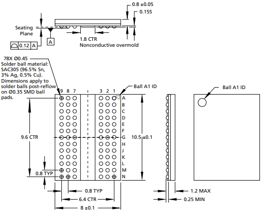
3. Package overview