Can ship immediately
Due to market price fluctuations,if you need to purchase or consult the price.You can contact us or emial to us: brenda@hongda-ic.com
1. Description
MT48LC32M16A2P-75:C is a high-speed CMOS dynamic random access memory, containing 536,870,912 bits. It is internally configured as four groups of DRAM with synchronous interfaces (all signals are registered on the positive edge of the clock signal CLK). Each of the 134,217,728-bit banks of x4 is organized as 8192 rows x 4096 columns x 4 Bit. Each of the 134,217,728-bit banks of x8 is organized into 8192 rows x 2048 columns It consists of 8 bits. Each of the 134,217,728-bit x16 banks is organized into 8192 rows x 1024 columns x 16 bits. Read and write access to SDRAM is burst-oriented; access starts from the selected Position and continue at the position of the programmed number in the programming sequence. The access starts with the registration of the ACTIVE command, followed by the READ or WRITE command. Registered address bit and The ACTIVE command is used to select the bank and row to be accessed (BA[1:0] select Bank; A[12:0] select line). The registered address bit is the same as READ or The WRITE command is used to select the starting column position of burst access. SDRAM provides programmable read or write burst length (BL) of 1, 2, 4 or 8 Position or full page, with burst termination option. Automatic pre-charging function Can be enabled to provide self-timed line pre-charging, which starts at the end Burst sequence. 512Mb SDRAM uses an internal pipeline architecture to achieve high-speed operation. This architecture is compatible with the 2n rule of the prefetch architecture, but it It also allows the column address to be changed every clock cycle to achieve high-speed, completely random access. Pre-charge another bank while visiting another bank The three banks will hide the PRECHARGE cycle and provide seamless, high-speed, random access operations. The 512Mb SDRAM is designed to run in a 3.3V storage system. Auto Refresh Provide modes, as well as power-saving and power-down modes. All inputs and outputs are compatible with LVTTL. SDRAM provides substantial improvements in DRAM operating performance, including Ability to synchronize burst data at high data rates through automatic column addresses Generation, the ability to stagger between internal banks to hide the pre-charge time, and The ability to randomly change the column address every clock cycle during the burst Right to use.
2. Feature
1. Compliant with PC100 and PC133
2. Fully synchronized; all signals are recorded in the active System clock edge
3. Internal pipeline operation; column address can be Change every clock cycle
4. Internal library for hidden row access/precharge
5. Programmable burst length: 1, 2, 4, 8 or full page
6. Automatic pre-charging, including concurrent automatic pre-charging And auto refresh mode
7. Self-refresh mode
8. Auto Refresh
– 64 milliseconds, 8192 periodic refresh (commercial and industrial)
9. LVTTL compatible input and output
10. Single 3.3V ±0.3V power supply
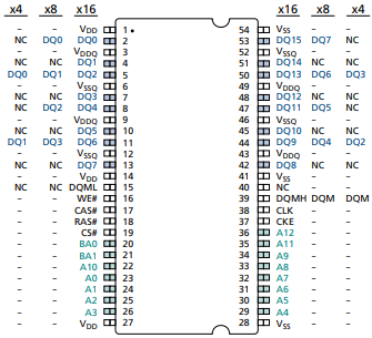
3. Pin configuration
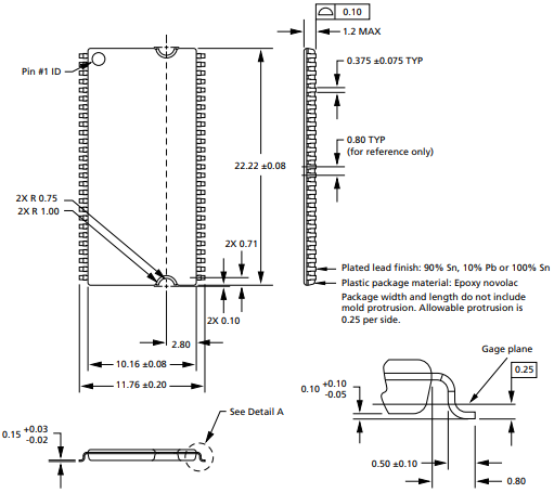
4. Package Dimensions