Can ship immediately
Due to market price fluctuations,if you need to purchase or consult the price.You can contact us or emial to us: brenda@hongda-ic.com
1. Description
The Micron® reduced latency DRAM (RLDRAM®) 2 is a high-speed memory device designed for high-bandwidth data storage such as telecommunications, networking, and cache applications. The chip’s 8-bank architecture is optimized for sustainable highspeed operation. The DDR I/O interface transfers two data words per clock cycle at the I/O balls. Output data is referenced to the free-running output data clock. Commands, addresses, and control signals are registered at every positive edge of the differential input clock, while input data is registered at both positive and negative edges of the input data clock(s). Read and write accesses to the device are burst-oriented. The burst length (BL) is programmable to 2, 4, or 8 by setting the mode register. The device is supplied with 2.5V and 1.8V for the core and 1.5V or 1.8V for the output drivers. Bank-scheduled refresh is supported with the row address generated internally. The 144-ball package is used to enable ultra high-speed data transfer rates and a simple upgrade path from early generation devices.
2. Features
1. 533 MHz DDR operation (1.067 Gb/s/pin data rate)
2. 38.4 Gb/s peak bandwidth (x36 at 533 MHz clock frequency)
3. Organization
– 32 Meg x 9, 16 Meg x 18, and 8 Meg x 36
4. 8 internal banks for concurrent operation and maximum bandwidth
5. Reduced cycle time (15ns at 533 MHz)
6. Nonmultiplexed addresses (address multiplexing option available)
7. SRAM-type interface
8. Programmable READ latency (RL), row cycle time, and burst sequence length
9. Balanced READ and WRITE latencies in order to optimize data bus utilization
10. Data mask for WRITE commands
11. Differential input clocks (CK, CK#)
12. Differential input data clocks (DKx, DKx#)
13. On-die DLL generates CK edge-aligned data and output data clock signals
14. Data valid signal (QVLD)
15. 32ms refresh (8K refresh for each bank; 64K refresh command must be issued in total each 32ms)
16. HSTL I/O (1.5V or 1.8V nominal)
17. 25–60Ω matched impedance outputs
18. 2.5V VEXT, 1.8V VDD, 1.5V or 1.8V VDDQ I/O
19. On-die termination (ODT) RTT
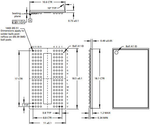
3. Package Dimensions