Can ship immediately
Due to market price fluctuations,if you need to purchase or consult the price.You can contact us or emial to us: brenda@hongda-ic.com
1. Describe
The MX25L6433FM2I-08G is a 64Mb-bit serial NOR flash with an internal configuration of 8,388,608 x 8. When it is in quad I/O mode, the structure becomes 16,777,216 bits x 4. When it is in two I/O mode, the structure becomes 33,554,432 bits x 2. The MX25L6433F has a serial peripheral interface and software protocol that allows a 3-wire bus in simple single I/O mode. The three bus signals are clock input (SCLK), serial data input (SI), and serial data output (SO). Enable serial access to the device via CS# input. MX25L6433F, MXSMIO® (Serial Multiple I/O) Flash, provides sequential read operations and multiple I/O capabilities to the entire chip. When it is in quad I/O mode, the SI pins, SO pins, WP# pins and HOLD# pins become SIO0 pins, SIO1 pins, SIO2 pins and SIO3 pins for address/ Virtual bit input and data input/output. After a program/erase command is issued, an automatic program/erase algorithm that programs/erases and verifies the specified page or sector/block location is executed. Program commands are executed in units of bytes or pages (256 bytes). Erase commands are performed on 4K-byte sectors, 32K-byte/64K-byte blocks, or the entire chip. In order to provide users with a convenient interface, a status register is included to indicate the status of the chip. The Status Read command can be issued through the WIP bit to detect the completion status of a program or erase operation. When the device is not running and CS# is high, it will remain in standby mode. The MX25L6433F uses Macronix's proprietary memory cells, which reliably store memory contents even after 100,000 program and erase cycles.
2. General
1. Serial Peripheral Interface Support - Mode 0 and Mode 3
2. 67,108,864 x 1-bit structure or 33,554,432 x 2-bit (two I/O read modes) or 16,777,216 x 4-bit (four I/O modes) structure
3. 2048 equal sectors of 4K bytes each - any sector can be individually erased
4. 256 equal blocks of 32K bytes each - any block can be individually erased
5. 128 equal blocks of 64K bytes each - any block can be individually erased
6. Power operation - 2.65-3.6 volts for read, erase and program operations
7. 100mA latch-up protection current from -1V to Vcc +1V
8. Support for performance-enhanced mode - XIP (execute in place)
3. Software function
1. Input data format
- 1 byte command code
2. Advanced security features
- Block lock protection BP0-BP3 and T/B status bits define the size of the area to be protected against program and erase instructions
3. Additional 8K-bit secure OTP - with unique identifier - factory lock identifiable, customer lockable
4. Auto Erase and Auto Program Algorithms - Automatically erase and verify selected data department
- Automatically program and validate data on selection
- Paging is automatically timed by an internal algorithm to program pulse width
5. Status register function
6. command reset
7. Program/Erase Suspend
8. Program/Erase Recovery
9. Electronic identification
- JEDEC 1-byte manufacturer ID and 2-byte device ID - RES command for 1-byte device ID
10. Supports Serial Flash Discoverable Parameter (SFDP) mode
4. Hardware Features
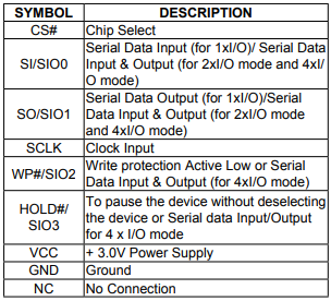
1. SCLK input
- Serial clock input
2. SI/SIO0
- 2 x serial data input or serial data input/output in I/O mode or 4 x serial data input/output in I/O mode
3. SO/SIO1
- 2 x Serial Data Out in I/O Mode or Serial Data In/Out or 4 x Serial Data In/Out in I/O Mode
4. WP#/SIO2
- 4 x I/O modes for hardware write protection or serial data input/output
5. Hold #/SIO3
- Suspend the device without deselecting the device or serial data input/output in 4 x I/O mode
6. Package
- 8-pin SOP (200mil)
- 16-pin SOP (300mil)
- 8-WSON (6x5mm)
- 8-WSON (8x6mm)
- 24-ball TFBGA (6x8mm)
- All devices are RoHS compliant and halogen free
5. Pin configuration

6. Pin Description
