
Can ship immediately
Due to market price fluctuations,if you need to purchase or consult the price.You can contact us or emial to us: brenda@hongda-ic.com
1. Device Description
The N25Q128A11ESF40G is the first high-performance multiple input/output serial Flash memory device manufactured on 65nm NOR technology. It features execute-in-place (XIP) functionality, advanced write protection mechanisms, and a high-speed SPI-compatible bus interface. The innovative, high-performance, dual and quad input/output instructions enable double or quadruple the transfer bandwidth for READ and PROGRAM operations.
2. Features
1. SPI-compatible serial bus interface
2. 108 MHz (MAX) clock frequency
3. 1.7–2.0V single supply voltage
4. Dual/quad I/O instruction provides increased throughput up to 432 MHz
5. Supported protocols
– Extended SPI, dual I/O, and quad I/O
6. Execute-in-place (XIP) mode for all three protocols
– Configurable via volatile or nonvolatile registers
– Enables memory to work in XIP mode directly after power-on
7. PROGRAM/ERASE SUSPEND operations
8. Continuous read of entire memory via a single command
– Fast read
– Quad or dual output fast read
– Quad or dual I/O fast read
9. Flexible to fit application
– Configurable number of dummy cycles
– Output buffer configurable
10. Software reset
11. 64-byte, user-lockable, one-time programmable (OTP) dedicated area
12. Erase capability
– Subsector erase 4KB uniform granularity blocks
– Sector erase 64KB uniform granularity blocks
– Full-chip erase
13. Write protection
– Software write protection applicable to every 64KB sector via volatile lock bit
– Hardware write protection: protected area size defined by five nonvolatile bits (BP0, BP1, BP2, BP3, and TB)
– Additional smart protections, available upon request
14. Electronic signature
– JEDEC-standard 2-byte signature (BB18h)
– Unique ID code (UID): 17 read-only bytes, including:
15. Two additional extended device ID (EDID) bytes to identify device factory options
16. Customized factory data (14 bytes)
17. Minimum 100,000 ERASE cycles per sector
18. More than 20 years data retention
19. Packages JEDEC standard, all RoHS compliant
– F7 = V-PDFN-8 6mm x 5mm Sawn (MLP8 6mm x 5mm)
– F8 = V-PDFN-8 8mm x 6mm (MLP8 8mm x 6mm)
– 12 = T-PBGA-24b05 6mm x 8mm
– SF = SOP2-16 300 mils body width (SO16W)
– SE = SOP2-8 208 mils body width (SO8W)
3. Pin configuration
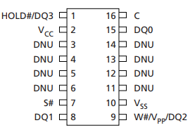
4. Device Configurability
The N25Q family offers additional features that are configured through the nonvolatile configuration register for default and/or nonvolatile settings. Volatile settings can be configured through the volatile and volatile-enhanced configuration registers. These configurable features include the following:
1. Number of dummy cycles for the fast READ commands
2. Output buffer impedance
3. SPI protocol types (extended SPI, DIO-SPI, or QIO-SPI)
4. Required XIP mode
5. Enabling/disabling HOLD (RESET function)
6. Enabling/disabling wrap mode

