Can ship immediately
Due to market price fluctuations,if you need to purchase or consult the price.You can contact us or emial to us: brenda@hongda-ic.com
1. Describe
The PCA9555PW,118 is a 24-pin CMOS device that provides 16-bit general purpose parallel input/output (GPIO) expansion for I2C-bus/SMBus applications and is designed to enhance NXP Semiconductors' family of I2C-bus I/O expanders. Improvements Includes higher drive capability, 5 V I/O tolerance, lower supply current, separate I/O configuration and smaller package. When additional I/O is required for ACPI power switches, sensors, buttons, LEDs, fans, etc., I/O expanders provide an easy solution. The PCA9555 consists of two 8-bit configuration (input or output select); input, output and polarity inversion (active high or active low operation) registers. The system host can enable I/O as input or output by writing to the I/O configuration bits. The data for each input or output is stored in the corresponding input or output register. The polarity of the read register can be reversed by the polarity inversion register. All registers can be read by the system host. Although pin-to-pin and I2C bus addresses are compatible with the PCF8575, application note AN469 discusses this due to enhancements that require changing software. The PCA9555 open-drain interrupt output is activated when any input state differs from it The corresponding input port register state indicates to the system host that the input state has changed. A power-on reset sets the registers to their default values and initializes the device state machine. Three hardware pins (A0, A1, A2) change the fixed I2C bus address and allow up to 8 devices to share the same I2C bus/SMBus. The PCA9555 has the same fixed I2C bus address as the PCA9554, allowing up to 8 of these devices in any combination to share the same I2C bus/SMBus.
2. Features
1. Operating supply voltage range is 2.3 V to 5.5 V
2. 5 V tolerant I/O
3. Polarity Inversion Register
4. Active low interrupt output
5. Low standby current
6. Noise filter on SCL/SDA input
7. Power on without fault
8. Internal power-on reset
9. 16 I/O pins, default 16 inputs
10. 0 Hz to 400 kHz clock frequency
11. ESD protection over 2000 V HBM per JESD22-A114, 200 V MM per JESD22-A115 and 1000 V CDM per JESD22-C101
12. Latch-up tested to over 100 mA per JEDEC standard JESD78
13. Available in five packages: SO24, SSOP24, TSSOP24, HVQFN24 and HWQFN24
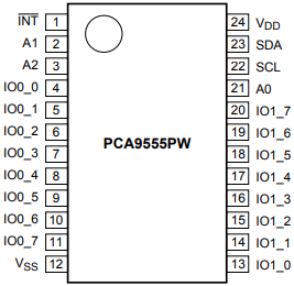
3. Pin configuration

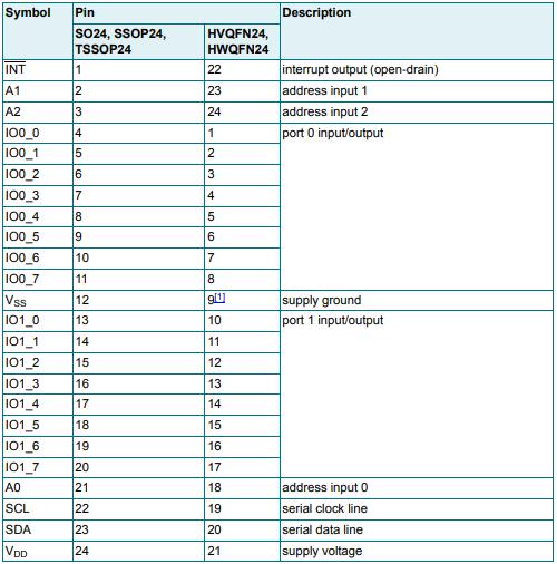
4. Pin Description

5. Acknowledge
The number of data bytes transferred between the START and the STOP conditions from transmitter to receiver is not limited. Each byte of eight bits is followed by one acknowledge bit. The acknowledge bit is a HIGH level put on the bus by the transmitter, whereas the master generates an extra acknowledge related clock pulse. A slave receiver which is addressed must generate an acknowledge after the reception of each byte. Also a master must generate an acknowledge after the reception of each byte that has been clocked out of the slave transmitter. The device that acknowledges has to pull down the SDA line during the acknowledge clock pulse, so that the SDA line is stable LOW during the HIGH period of the acknowledge related clock pulse; set-up time and hold time must be taken into account. A master receiver must signal an end of data to the transmitter by not generating an acknowledge on the last byte that has been clocked out of the slave. In this event, the transmitter must leave the data line HIGH to enable the master to generate a STOP condition.
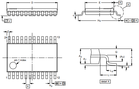
6. Product packaging
