Can ship immediately
Due to market price fluctuations,if you need to purchase or consult the price.You can contact us or emial to us: brenda@hongda-ic.com
1. Describe
SI4133-D-GT is a monolithic integrated circuit that can perform IF and dual-frequency radio frequency synthesis for wireless communication applications. The Si4133 includes three VCOs, loop filters, reference and VCO dividers, and phase detectors. The voltage divider and power-off settings can be programmed via a three-wire serial interface.
2. Feature
1. Dual frequency radio frequency synthesizer
- RF1: 900 MHz to 1.8 GHz
- RF2: 750 MHz to 1.5 GHz
2. Intermediate frequency synthesizer
- Intermediate frequency: 62.5 to 1000 MHz
3. Integrated VCO, loop filter, varactor diode and resonator
4. At least (2) external components required
5. Low phase noise
6. Programmable shutdown mode
7. 1 µA standby current
8. 18 mA typical supply current
9. 2.7 to 3.6 V operation
10. Package: 24-pin TSSOP, 28-pin QFN
- Lead-free and RoHS compliant
3. Application
1. Dual frequency communication
2. Digital mobile phone GSM 850, E-GSM 900, DCS 1800, PCS 1900
3. Digital cordless phone
4. Analog cordless phone
5. Wireless local loop
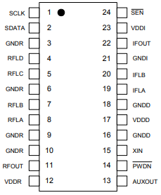
4. Pin configuration

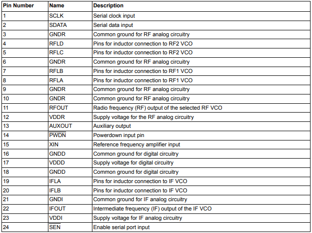
5. Pin description

6. Functional Description
The SI4133-D-GT is a monolithic integrated circuit that performs IF and dual-band RF synthesis for wireless communications applications. This integrated circuit (IC), with minimal external components, completes the frequency synthesis function necessary for RF communications systems. The Si4133 has three complete phase-locked loops (PLLs) with integrated voltage-controlled oscillators (VCOs). The low phase noise of the VCOs makes the Si4133 suitable for demanding wireless communications applications. Phase detectors, loop filters, and reference and output frequency dividers are integrated. The IC is programmed with a three-wire serial interface. Two PLLs are provided for dual-band RF synthesis. These RF PLLs are multiplexed so that only one PLL is active at a time, as determined by the setting of an internal register. The active PLL is the last one to be written. The center frequency of the VCO in each PLL is set by the value of an external inductance. Inaccuracies in these inductances are compensated for by the selftuning algorithm. The algorithm is run after powerup or after a change in the programmed output frequency. Each RF PLL, when active, can adjust the RF output frequency by ±5% of its VCO’s center frequency. Because the two VCOs can be set to have widely separated center frequencies, the RF output can be programmed to service two widely separated frequency bands by programming the corresponding N-Divider. One RF VCO is optimized to have its center frequency set between 947 MHz and 1.72 GHz, while the second RF VCO is optimized to have its center frequency set between 789 MHz and 1.429 GHz. One PLL is provided for IF frequency synthesis. The center frequency of this circuit’s VCO is set by the connection of an external inductance. The PLL can adjust the IF output frequency by ±5% of the VCO center frequency. Inaccuracies in the value of the external inductance are compensated for by the Si4133’s proprietary self-tuning algorithm. This algorithm is initiated each time the PLL is powered-up (by either the PWDN pin or by software) and/or each time a new output frequency is programmed. The IF VCO can have its center frequency set as low as 526 MHz and as high as 952 MHz. An IF output divider divides down the IF output frequencies, if needed. The divider is programmable and is capable of dividing by 1, 2, 4, or 8. The unique PLL architecture used in the Si4133 produces settling (lock) times that are comparable in speed to fractional-N architectures without the high phase noise or spurious modulation effects often associated with those designs.