Can ship immediately
Due to market price fluctuations,if you need to purchase or consult the price.You can contact us or emial to us: brenda@hongda-ic.com
1. Description
The SN65HVD485EDR device is a half-duplex transceiver designed for RS-485 data bus networks. Powered by a 5-V supply, it is fully compliant with the TIA/EIA-485A standard. This device is suitable for data transmission up to 10 Mbps over long twisted- pair cables and is designed to operate with very low supply current, typically less than 2 mA, exclusive of the load. When the device is in the inactive shutdown mode, the supply current drops below 1 mA. The wide common-mode range and high ESD protection levels of this device make it suitable for demanding applications such as: electrical inverters, status/command signals across telecom racks, cabled chassis interconnects, and industrial automation networks where noise tolerance is essential. The SN65HVD485E device matches the industry-standard footprint of the SN75176 device. Power-on reset circuits keep the outputs in a high- impedance state until the supply voltage has stabilized. A thermal-shutdown function protects the device from damage due to system-fault conditions. The SN65HVD485E device is characterized for operation from –40°C to 85°C air temperature.
2. Features
1. Bus-Pin ESD Protection up to 15 kV
2. 1/2 Unit Load: up to 64 Nodes on a Bus
3. Bus-Open-Failsafe Receiver
4. Glitch-Free Power-Up and Power-Down Bus Inputs and Outputs
5. Available in Small VSSOP-8 Package
6. Meets or Exceeds the Requirements of the TIA/EIA-485A Standard
7. Industry-Standard SN75176 Footprint
3. Applications
1. Motor Control
2. Power Inverters
3. Industrial Automation
4. Building Automation Networks
5. Industrial Process Control
6. Battery-Powered Applications
7. Telecommunications Equipment
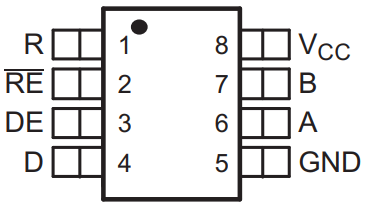
4. Pin Configuration

5. Pin Functions

6. Feature Description
The SN65HVD485EDR device provides internal biasing of the receiver input thresholds for open-circuit, bus-idle, or short-circuit failsafe conditions. It features a typical hysteresis of 30 mV to improve noise immunity. Internal ESD protection circuits protect the transceiver bus terminals against ±15-kV Human Body Model (HBM) electrostatic discharges.
7. Device Functional Modes
When the driver enable pin (DE) is logic high, the differential outputs A and B follow the logic states at data input D. A logic high at D causes A to turn high and B to turn low. In this case, the differential output voltage defined as VOD = VA – VB is positive. When D is low, the output states reverse, B turns high, A is low, and VOD is negative. When DE is low, both outputs turn high impedance. In this condition, the logic state at D is irrelevant. The DE pin has an internal pulldown resistor to ground; thus when left open, the driver is disabled (high impedance) by default. The D pin has an internal pullup resistor to VCC; thus when left open while the driver is enabled, output A turns high and B turns low. When the receiver enable pin (RE) is logic low, the receiver is enabled. When the differential input voltage defined as VID = VA – VB is positive and higher than the positive input threshold (VIT+) the receiver output (R) turns high. When VID is negative and lower than the negative input threshold (VIT– ), the receiver output (R) turns low. If VID is between VIT+ and VIT– , the output is indeterminate. When RE is logic high or left open, the receiver output is high impedance and the magnitude and polarity of VID are irrelevant. Internal biasing of the receiver inputs causes the output to go failsafe high when the transceiver is disconnected from the bus (open-circuit), the bus lines are shorted (short-circuit), or the bus is not actively driven (idle bus).
8. Typical Application
Receiver failsafe is accomplished by offsetting the receiver thresholds such that the input indeterminate range does not include zero volts differential. To comply with the RS-422 and RS-485 standards, the receiver output must output a high when the differential input VID is more positive than 200 mV, and it must output a Low when VID is more negative than –200 mV. The receiver parameters that determine the failsafe performance are VIT+, VIT– , and Vhys (the separation between VIT+ and VIT– ). As shown in the Electrical Characteristics: Receiver table, differential signals more negative than –200 mV cause a low receiver output, and differential signals more positive than 200 mV cause a high receiver output. When the differential input signal is close to zero, it is still above the VIT+ threshold, and the receiver output is High. Only when the differential input is more than Vhys below VIT+ does the receiver output transition to a Low state. Therefore, the noise immunity of the receiver inputs during bus fault conditions includes the receiver hysteresis value (Vhys) as well as the value of VIT+.