Can ship immediately
Due to market price fluctuations,if you need to purchase or consult the price.You can contact us or emial to us: brenda@hongda-ic.com
1. Describe
The SN65LVDS1, SN65LVDS2, and SN65LVDT2DBVR devices are single, low-voltage, differential line drivers and receivers in small-outline transistor packages. The outputs are TIA/EIA-644 compliant and provide a minimum differential output voltage amplitude of 247 mV into a 100 Ω load at signaling rates up to 630 Mbps for drivers and 400 Mbps for receivers. When the SN65LVDS1 device is used in a point-to-point connection with an LVDS receiver , data or clock signals can be transmitted through printed circuit board traces or cables at very high rates with very low electromagnetic radiation and power consumption. Packaging, low power consumption, low EMI, high ESD tolerance and wide supply voltage range make this device ideal for battery powered applications. The SN65LVDS1, SN65LVDS2, and SN65LVDT2DBVR devices have an operating temperature range of –40°C to 85°C.
2. Feature
1. Meets or exceeds ANSI TIA/EIA-644
2. Designed for signaling rates (1) up to:
– 630 Mbps driver
– Receiver 400 Mbps
3. Operates from a 2.4V to 3.6V supply
4. Available in SOT-23 and SOIC packages
5. Bus terminal ESD over 9 kV
6. Output voltage with typical low voltage differential signal of 350 mV into 100 Ω load
7. Propagation delay time
– 1.7ns typical drive
– 2.5ns typical receiver
8. Power consumption at 200 MHz
– 25 mW typical driver
– 60 mW typical receiver
9. LVDT receiver includes line termination
10. Low voltage TTL (LVTTL) level driver input 5V tolerant
11. Driver output high impedance, VCC < 1.5 V
12. Receiver output and input are high impedance, VCC < 1.5 V
13. Receiver open circuit fault protection
14. Differential input voltage threshold less than 100 mV
3. Application
1. Wireless infrastructure
2. Telecom infrastructure
4. Printer
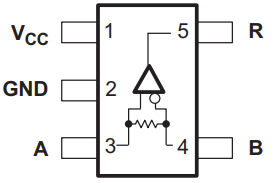
4. Pin configuration

5. Application Information
The SN65LVDS1, SN65LVDS2, and SN65LVDT2DBVR devices are single-channel LVDS buffers. The functionality of these devices is simple, yet so flexible that they can be used in designs ranging from wireless base stations to desktop computers. Different categories of potential applications share the features and applications discussed in the following paragraphs.