Can ship immediately
Due to market price fluctuations,if you need to purchase or consult the price.You can contact us or emial to us: brenda@hongda-ic.com
1. Describe
The SN74CBT16244CDLR is a high-speed TTL compatible FET bus switch with low on-resistance (ron) for minimal propagation delay. Active undershoot protection circuitry on the A and B ports of the SN74CBT16244C provides undershoot protection up to -2 V by detecting undershoot events and ensuring the switch remains in the correct off state. The SN74CBT16244C consists of four 4-bit bus switches with independent output enable (1OE, 2OE, 3OE, 4OE) inputs. It can be used as four 4-bit bus switches, two 8-bit bus switches or one 16-bit bus switch. When OE is low, the associated 4-bit bus switch is turned on and port A is connected to port B, allowing bidirectional data flow between ports. When OE is high, the associated 4-bit bus switch is turned off and a high impedance state exists between the A and B ports. The device is fully suitable for partial power down applications using Ioff. The Ioff function ensures that damage current does not flow back to the device when the device is powered off. The device features isolation in the event of a power outage. To ensure a high-impedance state on power-up or power-down, OE should be connected to VCC through a pull-up resistor; the minimum value of the resistor is determined by the current sink capability of the driver.
2. Feature
1. Texas Instruments Widebus TM Family Member
2. Undershoot protection for shutdown isolation of A and B ports up to −2 V
3. Bidirectional data flow with near-zero propagation delay
4. Low on-resistance (ron) characteristics (ron = 3 Ω typical)
5. Low input/output capacitance minimizes loading and signal distortion (Cio(OFF) = 5.5 pF typical)
6. Data and Control Inputs Provide Undershoot Clamping Diodes
7. Low power consumption (ICC = 3 µA Max)
8. VCC operating range is 4 V to 5.5 V
9. Data I/O supports 0 to 5-V signal levels (0.8-V, 1.2-V, 1.5-V, 1.8-V, 2.5-V, 3.3-V, 5-V)
10. Control inputs can be driven by TTL or 5V/3.3V CMOS outputs
11. Ioff supports partial power-down mode operation
12. Latch-up performance over 100 mA per JESD 78, Class II
13. ESD performance tested according to JESD 22
− 2000-V Human Body Model (A114-B, Class II)
− 1000V charging device model (C101)
14. Supports digital and analog applications: PCI interface, memory interleaving, bus isolation, low distortion signal gating
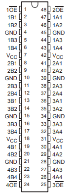
3. Pin configuration
