
Can ship immediately
Due to market price fluctuations,if you need to purchase or consult the price.You can contact us or emial to us: brenda@hongda-ic.com
1. Description
The TLV71310PQDBVRQ1 series of low-dropout (LDO) linear regulators are low quiescent current LDOs with excellent line and load transient performance and are designed for power-sensitive applications. These devices provide a typical accuracy of 1%. The TLV713P-Q1 series of devices is designed to be stable without an output capacitor. The removal of the output capacitor allows for a very small solution size. However, the TLV713P-Q1 series is also stable with any output capacitor if an output capacitor is used. The TLV713P-Q1 also provides inrush current control during device power-up and enabling. The TLV713P- Q1 limits the input current to the defined current limit to avoid large currents from flowing from the input power source. This functionality is especially important in battery-operated devices. The TLV713P-Q1 series is available in a standard DBV package and provides an active pulldown circuit to quickly discharge output loads. The TLV713P-Q1 is suited for automotive applications because the device is qualified for AEC-Q100 grade 1.
2. Features
1. AEC-Q100 Qualified with the Following Results:
– Device Temperature Grade 1: –40°C to 125°C Ambient Operating Temperature Range
– Device HBM ESD Classification Level H2
– Device CDM ESD Classification Level C4B
2. Input Voltage Range: 1.4 V to 5.5 V
3. Stable Operation With or Without Capacitors
4. Foldback Overcurrent Protection
5. Package: 5-Pin SOT-23
6. Very Low Dropout: 230 mV at 150 mA
7. Accuracy: 1%
8. Low IQ: 50 µA
9. Available in Fixed-Output Voltages:
– 1 V to 3.3 V
10. High PSRR: 65 dB at 1 kHz
11. Active Output Discharge
3. Applications
1. Automotive Head Units
2. Audio Amplifiers
3. DI Clusters
4. ADAS ECUs
5. Microprocessor Rails
6. USBs
7. Body Electronics
4. Pin Configurations
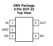
5. Pin Functions
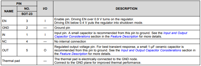
6. Feature Description
1. Undervoltage lockout (UVLO)
TLV713P-Q1 uses the UVLO circuit to disable the output until the input voltage is greater than the rise Undervoltage lockout voltage. This circuit ensures that the device will not exhibit any unpredictable behavior when it is powered The voltage is lower than the operating range of the internal circuit VIN(min). During the UVLO disabled period, the output TLV713P-Q1 is connected to ground through a 120Ω pull-down resistor.
2. Turn off
The enable pin (EN) is active high. The device is enabled by forcing the EN pin to exceed VEN (high) (0.9 V, minimum). Turn off the device by forcing the EN pin to drop below 0.4 V. If you don’t need to turn off the function, please connect to EN exist. TLV713P-Q1 has an internal pull-down MOSFET, when the device is in Disabled. Discharge time after disabling depends on output capacitance (COUT) and load resistance (RL) is connected in parallel with the 120Ω pull-down resistor.
3. Foldback current limit
The TLV713P-Q1 has an internal foldback current limit to help protect the regulator in the event of a fault. When the output voltage decreases, the current provided by the device gradually decreases. When the output is In the event of a short circuit, the LDO provides a typical current of 40 mA. The PMOS pass transistor dissipates [(VIN – VOUT) × ILIMIT] until thermal shutdown is triggered and the device turns off. The device is turned on by the internal thermal shutdown circuit during cooling. If the fault condition Continuing, the device cycles between current limit and thermal shutdown. The TLV713P-Q1 PMOS transmission element has a built-in body diode. When the OUT voltage is lower than The voltage at IN is exceeded. The current is not limited, so if the reverse voltage operation is expected to be extended, it is recommended to externally limit it to 5% of the rated output current.

