Can ship immediately
Due to market price fluctuations,if you need to purchase or consult the price.You can contact us or emial to us: brenda@hongda-ic.com
1. DESCRIPTION
The TPS2049D power-distribution switch is intended for applications where heavy capacitive loads and short circuits are likely to be encountered. This device incorporates a 600-mΩ N-channel MOSFET power switch for power-distribution systems that require only one power distribution path. The switch is controlled by a logic enable input. Gate drive is provided by an internal charge pump designed to control the power-switch rise times and fall times to minimize current surges during switching. The charge pump requires no external components and allows operation from supplies as low as 2.7V. When the output load exceeds the current-limit threshold or a short is present, the device limits the output current to a safe level by switching into a constant-current mode, pulling the overcurrent (OC) logic output low. When continuous heavy overloads and short circuits increase the power dissipation in the switch, causing the junction temperature to rise, a thermal protection circuit shuts off the switch to prevent damage. Recovery from a thermal shutdown is automatic once the device has cooled sufficiently. Internal circuitry ensures the switch remains off until valid input voltage is present. This power-distribution switch is designed to set current limit at 150mA typically.
2. FEATURES
1. 100-mA Continuous Current
2. 600-mΩ High-Side MOSFET
3. Thermal and Short-Circuit Protection
4. Operating Range: 2.7 V to 5.5 V
5. 0.6-ms Typical Rise Time
6. Undervoltage Lockout
7. Deglitched Fault Report (OC)
8. 43 µA Quiescent Supply Current
9. 1-µA Maximum Standby Supply Current
10. SOIC-8 Package
11. Ambient Temperature Range: –40°C to 85°C
12. 2 µS Response Time to Short Circuit
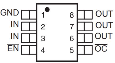
3. Pin configuration

4. Pin description

5. Function Description
1. switch
The power switch is an N-channel MOSFET with low on-resistance. The power switch is configured as a high-side switch, which prevents current from flowing from OUT to IN and IN to OUT when disabled. The minimum current provided by the power switch is 90 mA.
2. Charge pump
The internal charge pump powers the driver circuit and provides the necessary voltage to pull the gate of the MOSFET above the source. The charge pump works with input voltages as low as 2.7 V and requires very little supply current.
3. driver
The driver controls the gate voltage of the power switch. In order to limit the high current surge and reduce the related electromagnetic interference (EMI), the driver integrates a circuit that controls the rise time and fall time of the output voltage.
4. Enable (EN)
The logic enable pin disables the biasing of the power switch and charge pump, driver, and other circuits to reduce power supply current. When a logic high level appears on EN, the supply current will drop below 1 µA. The logic zero input on EN restores the bias of the drive and control circuit and opens the switch. Enable input is Compatible with TTL and CMOS logic levels.
5. Over current (OC)
When an overcurrent or overheating condition is encountered, the OC open-drain output is set (active low). The output remains active until the overcurrent or overheating condition is eliminated. The 10 millisecond deburring circuit can prevent the OC signal from oscillating or false triggering. Shut down if overheated When it happens, OC takes effect immediately.
6. Current sense
The sense FET monitors the current supplied to the load. Sensing FETs measure current more effectively than traditional resistance methods. When encountering an overload or short circuit, the current detection circuit will send a control signal to the driver. The driver in turn reduces the gate voltage and drives the power FET to its In the saturation zone, it switches the output to constant current mode and keeps the current constant while changing the load voltage.
7. Heat sensation
TPS2049 implements thermal sensing to monitor the operating temperature of the power distribution switch. In the case of overcurrent or short circuit, the junction temperature will rise. When the chip temperature rises to approximately 140°C due to overcurrent conditions, the internal thermal sensing circuit will close the switch, So as to prevent equipment damage. The hysteresis is built into the thermal induction, and the switch is turned on again after the device has cooled about 10 degrees. The switch continues to cycle off and on until the fault is eliminated. When overheating, the open-drain error report output (OC) is asserted (active low) A shutdown or overcurrent has occurred.
8. Undervoltage lockout
The voltage detection circuit monitors the input voltage. When the input voltage is lower than about 2V, the control signal will turn off the power switch.