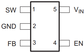
Can ship immediately
Due to market price fluctuations,if you need to purchase or consult the price.You can contact us or emial to us: brenda@hongda-ic.com
1. Describe
The TPS61041DBVRG4 is a high frequency boost converter Dedicated to small and medium LCD bias supply and White LED backlight power supply. The device is ideal Generates output voltages up to 28 V from dual batteries NiMH/NiCd or single cell Li-Ion battery. that part Can also be used to generate standard 3.3-V or 5-V to 12V power conversion. TPS61041DBVRG4 operates at switching frequency up to 1 MHz. This frequency allows the use of small external components using ceramic and Tantalum output capacitor. with the skinny WSON package, the TPS6104x provides a very small Overall solution size. The TPS61040 device has Internal 400-mA switch current limit, while The TPS61041 device has a switch current limit of 250mA, provides lower output voltage ripple and allows Use smaller size inductors to reduce power application. Low quiescent current (typically 28 μA) together with an optimized control scheme, Allows equipment to operate at very high efficiency the entire load current range.
2. Feature
1. 1.8V to 6V input voltage range
2. Adjustable output voltage range up to 28 V
3. 400mA (TPS61040) and 250mA (TPS61041) Internal switch current
4. Up to 1MHz switching frequency
5. 28μA typical no-load quiescent current
6. 1μA typical shutdown current
7. Internal soft start
8. Provide SOT23-5, TSOT23-5, and 2mm × 2mm × 0.8mm WSON package
3. Application
1. LCD bias supply
2. White LED power supply for LCD backlight
3. Digital camera
4. PDAs, managers and handheld PCs
5. cell phone
6. Internet Audio Player
7. Standard 3.3V or 5V to 12V conversion
4. Password configuration

5. Detailed description

6. Feature Description
1. Peak Current Control
The internal switch turns on until the inductor current reaches the typical dc current limit (ILIM) of 400 mA (TPS61040) or 250 mA (TPS61041). Due to the internal propagation delay of typical 100 ns, the actual current exceeds the dc current limit threshold by a small amount. By selecting the TPS6104x, it is possible to tailor the design to the specific application current limit requirements.A lower current limit supports applications requiring lower output power and allows the use of an inductor with a lower current rating and a smaller form factor. A lower current limit usually has a lower output voltage ripple as well.
2. Soft Start
All inductive step-up converters exhibit high inrush current during start-up if no special precaution is made. This can cause voltage drops at the input rail during start up and may result in an unwanted or early system shut down.
3. Enable
Pulling the enable (EN) to ground shuts down the device reducing the shutdown current to 1 μA (typical). Because there is a conductive path from the input to the output through the inductor and Schottky diode, the output voltage is equal to the input voltage during shutdown. The enable pin needs to be terminated and should not be left floating. Using a small external transistor disconnects the input from the output during shutdown as shown
4. Undervot
An undervoltage lockout prevents misoperation of the device at input voltages below typical 1.5 V. When the input voltage is below the undervoltage threshold, the main switch is turned off.
5. Thermal Shutdown
An internal thermal shutdown is implemented and turns off the internal MOSFETs when the typical junction temperature of 168°C is exceeded. The thermal shutdown has a hysteresis of typically 25°C. This data is based on statistical means and is not tested during the regular mass production of the IC.
7. Application Information
The TPS61041DBVRG4 are designed for output voltages up to 28V, with an input voltage range of 1.8V to 6V, and The switch peak current is limited to 400 mA (250 mA for the TPS61041). The device operates using a pulse frequency modulation (PFM) scheme with constant peak current control. This control scheme maintains high efficiency over Over the entire load current range, and switching frequencies up to 1 MHz, the device can be used very small external components. The following sections provide information for configuring TPS61040 Regulated Boost Converter as LCD Bias Supply
8. Device Functional Modes
The TPS61041DBVRG4 operates over an input voltage range of 1.8V to 6V and can generate output voltages up to 28V, V. The device operates using a pulse frequency modulation (PFM) scheme with constant peak current control. This control scheme maintains high efficiency over the entire load current range, and with switching frequencies up to 1 MHz, the device allows the use of very small external components. The converter monitors the output voltage, and once the feedback voltage falls below the reference voltage, typically 1.233 V, the internal switch turns on and the current ramps up. Once the switch is closed the inductor current reaches an internally set typical peak current of 400 mA (TPS61040) or 250 mA (TPS61041). The second criterion to turn off the switch is a maximum on-time of 6 μs (typ). This is just to limit the maximum on-time of the converter for extreme conditions. When the switch is closed, the external Schottky diode is forward biased, delivering current to the output. This switch remains off for at least 400 ns (typ), or until the feedback voltage drops below the reference voltage again. Using this PFM peak current control scheme, the converter operates in discontinuous conduction mode (DCM), where the switching frequency depends on the output current, so the efficiency is very high over the entire load current range. This regulation scheme is inherently stable, allowing a wider selection of inductors and output capacitors.