Can ship immediately
Due to market price fluctuations,if you need to purchase or consult the price.You can contact us or emial to us: brenda@hongda-ic.com
1. Describe
The TPS65263-1QRHBRQ1 contains a triple synchronous buck converter with a wide 4.0 to 18V input voltage. Converters with constant frequency peak current mode are designed to simplify their application while giving designers the option to optimize the system for the target application. The switching frequency of the converter is adjustable from 200 kHz to 2.3 MHz with external resistors. The 180° out-of-phase operation between buck1 and buck2, buck3 (buck2 and buck3 in-phase operation) minimizes input filter requirements. The initial start-up voltage for each buck can be programmed with external feedback resistors. The output voltage of the buck2 is dynamically adjustable from 0.68 to 1.95 V in 10 mV steps via an I2C controlled 7-bit VID. The VID voltage transition slew rate is programmable via the I2C bus with a 3-bit control to optimize overshoot/undershoot during VID voltage transitions. Each buck in the TPS65263-1Q1 can be controlled via I2C to enable/disable output voltage, set pulse skip mode (PSM) or forced continuous current (FCC) mode at light load conditions, and read power good, over- Flow warning and chip temperature warning. The TPS65263-1Q1 has overvoltage, overcurrent, short circuit and thermal protection functions.
2. Feature
1. Compliant with automotive application requirements
2. AEC-Q100 certification results are as follows:
– Device Temperature Grade 1: –40°C to 125°C Operating Junction Temperature Range
– Device HBM ESD classification level H2
– Equipment CDM ESD classification level C4B
3. Operating input voltage range 4.0 to 18V Maximum continuous output current 3 A/2 A/2 A
4. I2C controlled 7-bit VID programmable output voltage range from 0.68 to 1.95 V with 10 mV buck 2 step
5. I2C controlled VID voltage conversion slew rate for Buck2
6. I2C readback power good status, overcurrent warning and die temperature warning
7. I2C Compatible Interface with Standard Mode (100 kHz) and Fast Mode (400 kHz)
8. Feedback reference voltage 0.6 V ±1%
9. Adjustable clock frequency from 200 kHz to 2.3 MHz
10. FCC mode (default)
11. External clock synchronization
12. Dedicated enable and soft-start pins for each buck converter
13. Output voltage power good indicator
14. Thermal overload protection
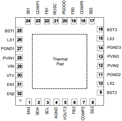
3. Pin configuration

4. Application
1. car
2. Car audio/video
3. Home gateway and access point networks
4. Monitoring
5. Serial Interface Description
I2C is a 2-wire serial interface developed by NXP Semiconductor (see I2C Bus Specification, Version 2.1, January 2000). The bus consists of a data line (SDA) and a clock line (SCL) with a pull-up structure. When the bus is idle, both the SDA and SCL lines are pulled high. all me 2C compatible devices are connected to the I2C bus through open-drain I/O pins, SDA and SCL. A master device (usually a microcontroller or digital signal processor) controls the bus. The host is responsible for generating the SCL signal and device address. Master also Generate specific conditions that indicate the start and stop of data transfers. A slave device receives and/or transmits data on the bus under the control of the master device. The TPS65263-1Q1 device operates as a slave and supports the following data transfer modes as defined in the I2C bus specification: standard mode (100 kbps) and fast mode (400 kbps). This interface adds flexibility to the power solution, allowing most functions to be programmed to new values based on transient application requirements. The register contents remain unchanged as long as the supply voltage remains above 3.8 V (typ). The data transfer protocols for standard mode and quick mode are exactly the same. Therefore, they are referred to as F/S modes in this document. The TPS65263-1Q1 device supports 7-bit addressing. 10-bit addressing and broadcast addresses are not supported.
6. Application Information
The device is a triple synchronous step-down DC/DC converter with I2C interface. it is usually used to convertConvert higher DC voltages to lower DC voltages with 3 A/2 A/2 A continuously available output current.