Can ship immediately
Describe
XC17128EPD8C series configuration PROM provides a An easy-to-use, cost-effective method for storing large Xilinx FPGA configuration bit stream. When the FPGA is in the master serial mode, it generates a The configuration clock that drives the PROM. Short visit The time after the rising edge of the clock, the data appears on the PROM Connect to the DATA output pin of the FPGA DIN pin. this FPGA generates an appropriate number of clock pulses to Complete the configuration. After configuration, it is disabled prom. When FPGA is in slave serial mode, PROM And the FPGA must be clocked by the input signal. Can use CEO to connect multiple devices Output to drive the CE input of the following devices. this Clock input and data output of all PROMs The chains are interrelated. All devices are compatible and Can be cascaded with other members of the family. For device programming, Xilinx Alliance or Foundation software compiles FPGA design files into a Standard hexadecimal format, then transmitted to most Commercial PROM programmer.
Features
1. One-time programmable (OTP) read-only memory designed to store configuration bitstreams of Xilinx® FPGAs
2. Simple interface to the FPGA; requires only one user I/O pin
3. Cascadable for storing longer or multiple bitstreams
4. Programmable reset polarity (active High or active Low) for compatibility with different FPGA solutions
5. XC17128E/EL, XC17256E/EL, XC1701, and XC1700L series support fast configuration
6. Low-power CMOS floating-gate process
7. XC1700E series are available in 5V and 3.3V versions
8. XC1700L series are available in 3.3V only
9. Available in compact plastic packages: 8-pin SOIC, 8-pin VOIC, 8-pin PDIP, 20-pin SOIC, 20-pin PLCC, 44-pin PLCC or 44-pin VQFP
10. Programming support by leading programmermanufacturers
11. Design support using the Xilinx Alliance and Foundation™ software packages
12. Guaranteed 20 year life data retention
13. Lead-free (Pb-free) packaging available
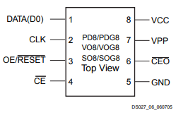
Pin configuration

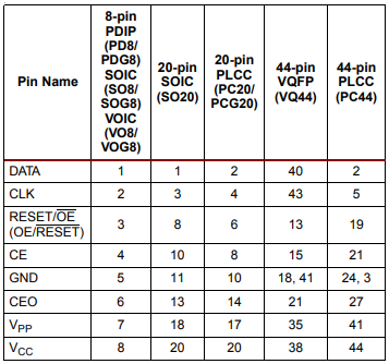
Pin Description
