
Can ship immediately
Due to market price fluctuations,if you need to purchase or consult the price.You can contact us or emial to us: brenda@hongda-ic.com
1. Describe
The Spartan®-6 series provides leading system integration functions for high-volume applications at the lowest total cost. this The 13-person series provides an expansion of the density from 3840 logic units to 147443 logic units, and the power consumption is only half of the previous The Spartan family, and faster and more comprehensive connections. Based on the mature 45nm low-power copper process technology, The Spartan-6 series provides the best balance of cost, power consumption and performance, providing a new and more efficient dual-register 6-input look-up table (LUT) logic and a wealth of built-in system-level module options. Including 18 Kb (2 x 9 Kb) RAM blocks, second generation DSP48A1 slice, SDRAM memory controller, enhanced mixed-mode clock management module, SelectIO™ technology, power optimized high-speed serial transceiver module, PCI Express® compatible endpoint module, advanced system-level power management Automatic detection mode, configuration options and enhanced IP security are protected by AES and Device DNA. These features provide a low-cost programmable alternative to custom ASIC products with unprecedented ease of use. Spartan-6 FPGA provides the best solution High-capacity logic design, consumer-oriented DSP design and cost-sensitive embedded applications. Spartan-6 FPGA Yes The programmable silicon foundation of the target design platform provides integrated software and hardware components to achieve Designers focus on innovation at the beginning of the development cycle.
2. Features
1. Spartan-6 family
-Spartan-6 LX FPGA: logic optimization
-Spartan-6 LXT FPGA: High-speed serial connection
2. Low cost design
-Multiple efficient integrated blocks
-Optimize the selection of I/O standards
-Staggered pads
-Large-capacity plastic wire bonding package
3. Low static and dynamic power consumption
-45nm process optimized for cost and low power consumption
-Sleep power-down mode to achieve zero power consumption
-Suspend mode through multi-pin wakeup, control enhancements to maintain state and configuration
-Low power consumption 1.0V core voltage (only LX FPGA, -1L)
-High performance 1.2V core voltage (LX and LXT FPGA, -2, -3 and -3N speed grades)
4. Multi-voltage, multi-standard SelectIO™ interface group
-The data transfer rate of each differential I/O is up to 1,080 Mb/s
-Optional output drive, up to 24 mA per pin
-3.3V to 1.2V I/O standards and protocols
-Low cost HSTL and SSTL memory interface
-Hot plug compliance
-Adjustable I/O conversion rate to improve signal integrity
5. High-speed GTP serial transceiver in LXT FPGA
-Up to 3.2 Gb/s
-High-speed interfaces include: Serial ATA, Aurora, 1G Ethernet, PCI Express, OBSAI, CPRI, EPON, GPON, DisplayPort and XAUI
6. Integrated Endpoint Module (LXT) for PCI Express design
7. Low-cost PCI® technical support, compatible with 33 MHz, 32-bit and 64-bit specifications.
8. Efficient DSP48A1 slice
-High-performance arithmetic and signal processing
-Fast 18 x 18 multiplier and 48-bit accumulator
-Pipeline and cascading capabilities
-Pre-adder for auxiliary filter application
9. Integrated memory controller module
-DDR, DDR2, DDR3 and LPDDR support
-Data rate up to 800 Mb/s (12.8 Gb/s peak bandwidth)
-Multi-port bus structure with independent FIFO to reduce design timing issues
10. Abundant logic resources and increased logic capacity
-Optional shift register or distributed RAM support
-Efficient 6-input LUT improves performance and minimizes power consumption
-LUT with dual triggers, suitable for pipeline-centric applications
11. Block RAM with a wide range of granularity
-Fast block RAM with byte write enable
-18 Kb blocks, can be selectively programmed as two independent 9 Kb blocks of RAM
12. Clock Management Tile (CMT) for enhanced performance
-Low noise, flexible clock
-Digital Clock Manager (DCM) can eliminate clock deviation and duty cycle distortion
-Phase-locked loop (PLL) for low jitter clock
-Simultaneous frequency synthesis of multiplication, division and phase shift
-16 low-skew global clock networks
13. Simplify configuration and support low-cost standards
-2-pin automatic detection configuration
-Extensive third-party SPI (up to x4) and NOR flash support
-Feature-rich Xilinx platform flash memory with JTAG
-MultiBoot supports multi-bit stream remote upgrade, using watchdog protection
14. Enhance the safety of design protection
-Unique Device DNA Identifier for design certification
-AES bitstream encryption in large equipment
15. Use enhanced low-cost MicroBlaze™ for faster embedded processing processor
16. Industry-renowned IP and reference designs feature
3. I/O Electrical Characteristics
Single-ended outputs use a conventional CMOS push/pull output structure, driving High towards VCCO or Low towards ground, and can be put into high-Z state. Many I/O features are available to the system designer to optionally invoke in each I/O in their design, such as weak internal pull-up and pull-down resistors, strong internal split-termination input resistors, adjustable output drive-strengths and slew-rates, and differential termination resistors. See the Spartan-6 FPGA SelectIO Resources User Guide for more details on available options for each I/O standard.
Function summary
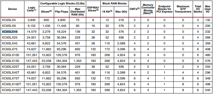
4. Configuration
Spartan-6 FPGAs store the customized configuration data in SRAM-type internal latches. The number of configuration bits is between 3 Mb and 33 Mb depending on device size and user-design implementation options. The configuration storage is volatile and must be reloaded whenever the FPGA is powered up. This storage can also be reloaded at any time by pulling the PROGRAM_B pin Low. Several methods and data formats for loading configuration are available. Bit-serial configurations can be either master serial mode, where the FPGA generates the configuration clock (CCLK) signal, or slave serial mode, where the external configuration data source also clocks the FPGA. For byte-wide configurations, master SelectMAP mode generates the CCLK signal while slave SelectMAP mode receives the CCLK signal for the 8- and 16-bit-wide transfer. In master serial mode, the beginning of the bitstream can optionally switch the clocking source to an external clock, which can be faster or more precise than the internal clock. The available JTAG pins use boundary-scan protocols to load bit-serial configuration data. The bitstream configuration information is generated by the ISE® software using a program called BitGen. Configuration The process usually executes the following sequence:
1. Detect power-on (power-on reset) or PROGRAM_B at low level.
2. Clear the entire configuration memory.
3. The sampling mode pin determines the configuration mode: master or slave, bit serial or parallel.
4. Load the configuration data from the bus width detection mode, followed by the synchronization word, check It is used for the correct device code and ends with a cyclic redundancy check (CRC) of the complete bitstream.
5. Start a user-defined sequence of events: release the internal reset (or preset) of the trigger, choose to wait The DCM and/or PLL lock, activate the output driver, and switch the DONE pin to a high level.
Master Serial Peripheral Interface (SPI) and Master Byte-wide Peripheral Interface (BPI) are two commonly used methods Used to configure the FPGA. The Spartan-6 FPGA configures itself via a direct- connected industry standard SPI serial Flash PROM. When Spartan-6 FPGA is connected to industry standard parallel NOR flash memory, it can configure itself through BPI. Please note that XC6SLX4, XC6SLX25 and XC6SLX25T do not support BPI configuration, use Spartan-6 FPGA in TQG144 and CPG196 packages. Spartan-6 FPGA supports MultiBoot configuration, where two or more FPGA configuration bitstreams can be stored in one Single configuration source. The FPGA application controls which configuration is loaded next and when it is loaded. The Spartan-6 FPGA also includes a unique, factory-programmed Device DNA identifier, which can be used for tracking purposes, anti-clone design, or IP protection. In the largest devices, the bitstream can be copy protected using AES encryption.

