Can ship immediately
Due to market price fluctuations,if you need to purchase or consult the price.You can contact us or emial to us: brenda@hongda-ic.com
1. Operating Conditions
1. 2.7V – 5.5V, -40°C to +125°C, DC to 48 MHz
2. Core
1. Arm® Cortex®-M0+ CPU running at up to 48 MHz:
– Single-cycle hardware multiplier
– Micro Trace Buffer
– Memory Protection Unit (MPU)
3. Memories
1. 32/64/128/256 KB in-system self-programmable Flash
2. 1/2/4/8 KB independent self-programmable Flash for EEPROM emulation
3. 4/8/16/32 KB SRAM Main Memory
4. System
1. Power-on Reset (POR) and Brown-out Detection (BOD)
2. Internal and external clock options with 48 MHz to 96 MHz Fractional Digital Phase Locked Loop (FDPLL96M)
3. External Interrupt Controller (EIC) (Interrupt pin debouncing is only available in SAM C20/C21 N)
4. 16 external interrupts
– Hardware debouncing (only available in SAM C20/C21 N)
5. One non-maskable interrupt
6. Two-pin Serial Wire Debug (SWD) programming, test, and debugging interface
5. Low-Power
1. Idle and Standby Sleep modes
2. SleepWalking peripherals
6. Peripherals
1. Hardware Divide and Square Root Accelerator (DIVAS)
2. 12-channel Direct Memory Access Controller (DMAC)
3. 12-channel Event System
4. Up to eight 16-bit Timer/Counters (TC), configurable as either:
– Maximum and minimum capture is only available in the SAM C21N devices.
– One 16-bit TC with compare/capture channels
– One 8-bit TC with compare/capture channels
– One 32-bit TC with compare/capture channels, by using two TCs
5. Two 24-bit and one 16-bit Timer/Counter for Control (TCC), with extended functions:
– Up to eight PWM channels on each 24-bit TCC
– Up to two PWM channels on each 16-bit TCC
– Up to four compare channels with optional complementary output
– Generation of synchronized pulse width modulation (PWM) pattern across port pins
– Deterministic fault protection, fast decay and configurable dead-time between complementary output
– Dithering that increase resolution with up to 5 bit and reduce quantization error
6. Frequency Meter (The division reference clock is only available in the SAM C21N)
7. 32-bit Real Time Counter (RTC) with clock/calendar function
8. Watchdog Timer (WDT)
9. CRC-32 generator
10. Up to two Controller Area Network (CAN) interfaces in the SAM C21:
– CAN 2.0A/B and CAN-FD (ISO 11898-1:2015)
11. Each CAN interface have two selectable pin locations to switch between two external CAN transceivers (without the need for an external switch)
12. Up to eight Serial Communication Interfaces (SERCOM), each configurable to operate as either:
– USART with full-duplex and single-wire half-duplex configuration
– I2C up to 3.4 MHz (Except SERCOM6 and SERCOM7)
– SPI
– LIN host/client
– RS-485
– PMBus
13. One Configurable Custom Logic (CCL)
14. Up to Two 12-bit, 1 Msps Analog-to-Digital Converter (ADC) with up to 12 channels each (20 unique channels)
– Differential and single-ended input
– Automatic offset and gain error compensation
– Oversampling and decimation in hardware to support 13, 14, 15 or 16-bit resolution
15. One 16-bit Sigma-Delta Analog-to-Digital Converter (SDADC) with up to 3 differential channels in the SAM C21
16. 10-bit, 350 ksps Digital-to-Analog Converter (DAC) in the SAM C21
17. Up to four Analog Comparators (AC) with Window Compare function
18. Integrated Temperature Sensor in the SAM C21
19. Peripheral Touch Controller (PTC)
– 256-Channel capacitive touch and proximity sensing
7. Describe
When enabled, MTB will record changes in the program flow and report them by the Cortex-M0+ processor during execution Tracking interface shared between Cortex-M0+ processor and CoreSight MTB-M0+. Information is stored As the trace data packet of MTB in SRAM. Off-chip debugger can use Debug The access port reads trace information from SRAM. Then the debugger can rebuild the program flow This information. MTB also stores trace information in SRAM and allows the processor to access SRAM. this MTB ensures that tracking write access takes precedence over processor access. The execution trace packet consists of a pair of 32-bit words and is generated when the MTB detects the processor The PC value changes randomly. Non-sequential PC change exception entries may occur during branch instructions or during execution. When the MASTER.EN bit in the master tracking control register is 1, the tracking is enabled. There are multiple setting methods This bit is 1 to start tracking, or 0 to stop tracking. Mountain bike can It is programmed to automatically stop tracking or start or stop when the memory is filled to the specified watermark level Tracking is performed by directly writing to the MASTER.EN bit. If the watermarking mechanism is not used and the trace buffer overflows, the buffer will wrap around and overwrite the previous trace data packet. The base address of the MTB register is 0x41008000; this address is also written into the CoreSight ROM table. The offset of each register relative to the base address is fixed and is manually defined by the CoreSight MTB-M0+ technical reference. MTB has 4 programmable registers to control the behavior of the tracking function:
1. POSITION: Contains tracking write pointer and line feed bit,
2. MASTER: Contains the main tracking enable bit and other tracking control fields,
3. FLOW: Contains the WATERMARK address and AUTOSTOP and AUTOHALT control bits,
4. BASE: Indicates the location of SRAM in the processor memory map. This register is used to enable The MTB SRAM location is automatically discovered by the debugging agent.
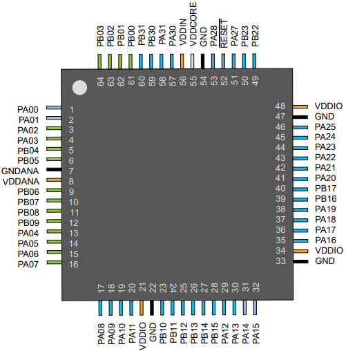
8. Pin configuration
