Can ship immediately
The C8051F12x and C8051F13x device families are fully integrated mixed-signal System-on-a-Chip MCUs with 64 digital I/O pins (100-pin TQFP) or 32 digital I/O pins (64-pin TQFP).
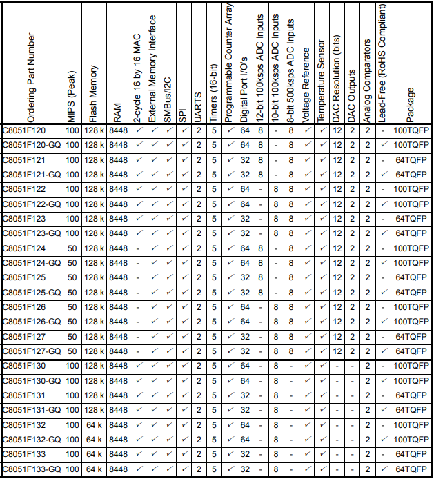
Highlighted features are listed below. Refer to Table 1.1 for specific product feature selection.
1. High-Speed pipelined 8051-compatible CIP-51 microcontroller core (100 MIPS or 50 MIPS)
2. In-system, full-speed, non-intrusive debug interface (on-chip)
3. True 12 or 10-bit 100 ksps ADC with PGA and 8-channel analog multiplexer
4. True 8-bit 500 ksps ADC with PGA and 8-channel analog multiplexer (C8051F12x Family)
5. Two 12-bit DACs with programmable update scheduling (C8051F12x Family)
6. 2-cycle 16 by 16 Multiply and Accumulate Engine (C8051F120/1/2/3 and C8051F130/1/2/3)
7. 128 or 64 kB of in-system programmable Flash memory
8. 8448 (8 k + 256) bytes of on-chip RAM
9. External Data Memory Interface with 64 kB address space
10. SPI, SMBus/I2C, and (2) UART serial interfaces implemented in hardware
11. Five general purpose 16-bit Timers
12. Programmable Counter/Timer Array with 6 capture/compare modules
13. On-chip Watchdog Timer, VDD Monitor, and Temperature Sensor
With on-chip VDD monitor, Watchdog Timer, and clock oscillator, the C8051F12x and C8051F13x devices are truly stand-alone System-on-a-Chip solutions. All analog and digital peripherals are enabled/disabled and configured by user firmware. The Flash memory can be reprogrammed even in-circuit, providing nonvolatile data storage, and also allowing field upgrades of the 8051 firmware.
On-board JTAG debug circuitry allows non-intrusive (uses no on-chip resources), full speed, in-circuit debugging using the production MCU installed in the final application. This debug system supports inspection and modification of memory and registers, setting breakpoints, watchpoints, single stepping, run and halt commands. All analog and digital peripherals are fully functional while debugging using JTAG.
Each MCU is specified for operation over the industrial temperature range (–45 to +85 °C). The Port I/O, RST, and JTAG pins are tolerant for input signals up to 5 V. The devices are available in 100-pin TQFP or 64-pin TQFP packaging. Table 1.1 lists the specific device features and package offerings for each part number. Figure 1.1 through Figure 1.6 show functional block diagrams for each device.
