Can ship immediately
Due to market price fluctuations,if you need to purchase or consult the price.You can contact us or emial to us: brenda@hongda-ic.com
1. Description
The CD4051BM analog multiplexers and demultiplexers are digitally-controlled analog switches having low ON impedance and very low OFF leakage current. These multiplexer circuits dissipate extremely low quiescent power over the full VDD – VSS and VDD – VEE supply-voltage ranges, independent of the logic state of the control signals.
2. Features
1. Wide Range of Digital and Analog Signal Levels
– Digital: 3 V to 20 V
– Analog: ≤ 20 VP-P
2. Low ON Resistance, 125 Ω (Typical) Over 15 VP-P Signal Input Range for VDD – VEE = 18 V
3. High OFF Resistance, Channel Leakage of ±100 pA (Typical) at VDD – VEE = 18 V
4. Logic-Level Conversion for Digital Addressing Signals of 3 V to 20 V (VDD – VSS = 3 V to 20 V) to Switch Analog Signals to 20 VP-P (VDD – VEE = 20 V) Matched Switch Characteristics, rON = 5 Ω (Typical) for VDD – VEE = 15 V Very Low Quiescent Power Dissipation Under All Digital-Control Input and Supply Conditions, 0.2 µW (Typical) at VDD – VSS = VDD – VEE = 10 V
5. Binary Address Decoding on Chip
6. 5 V, 10 V, and 15 V Parametric Ratings
7. 100% Tested for Quiescent Current at 20 V
8. Maximum Input Current of 1 µA at 18 V Over Full Package Temperature Range, 100 nA at 18 V and 25°C
9. Break-Before-Make Switching Eliminates Channel Overlap
3. Applications
1. Analog and Digital Multiplexing and Demultiplexing
2. A/D and D/A Conversion
3. Signal Gating
4. Factory Automation
5. Televisions
6. Appliances
7. Consumer Audio
8. Programmable Logic Circuits
9. Sensors
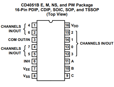
4. Pin Configuration and Functions

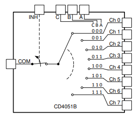
5. Functional Diagrams of CD4051BM

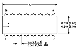
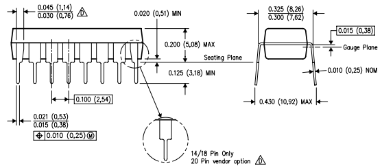
6. Packaging Information

