Can ship immediately
Due to market price fluctuations,if you need to purchase or consult the price.You can contact us or emial to us: brenda@hongda-ic.com
1. Describe
MC9S08AW60CFUE, MC9S08AW48, MC9S08AW32 and MC9S08AW16 are low-cost, high-performance HCS08 series 8-bit microcontroller units (MCU). All MCUs in this series use the enhanced HCS08 core, which can be used for various modules, memory sizes, memory types, and package types. About memory size and package type.
2. Features
1. 8-Bit HCS08 Central Processor Unit (CPU)
- 40-MHz HCS08 CPU (central processor unit)
- 20-MHz internal bus frequency
- HC08 instruction set with added BGND instruction
- Single-wire background debug mode interface
- Breakpoint capability to allow single breakpoint setting during in-circuit debugging (plus two more breakpoints in on-chip debug module)
- On-chip real-time in-circuit emulation (ICE) with two comparators (plus one in BDM), nine trigger modes, and on-chip bus capture buffer. Typically shows approximately 50 instructions before or after the trigger point.
- Support for up to 32 interrupt/reset sources
2. Memory Options
- Up to 60 KB of on-chip in-circuit programmable FLASH memory with block protection and security options
- Up to 2 KB of on-chip RAM
3. Clock Source Options
- Clock source options include crystal, resonator, external clock, or internally generated clock with precision NVM trimming
4. System Protection
- Optional computer operating properly (COP) reset
- Low-voltage detection with reset or interrupt
- Illegal opcode detection with reset
- Illegal address detection with reset (some devices don’t have illegal addresses)
5. Power-Saving Modes
- Wait plus two stops
6. Peripherals
- ADC — Up to 16-channel, 10-bit analog-to-digital converter with automatic compare function
- SCI — Two serial communications interface modules with optional 13-bit break
- SPI — Serial peripheral interface module
- IIC — Inter-integrated circuit bus module to operate at up to 100 kbps with maximum bus loading; capable of higher baud rates with reduced loading
- Timers — One 2-channel and one 6-channel 16-bit timer/pulse-width modulator (TPM) module: Selectable input capture, output compare, and edge-aligned PWM capability on each channel. Each timer module may be configured for buffered, centered PWM (CPWM) on all channels
- KBI — Up to 8-pin keyboard interrupt module
7. Input/Output
- Up to 54 general-purpose input/output (I/O) pins
- Software-selectable pullups on ports when used as inputs
- Software-selectable slew rate control on ports when used as outputs
- Software-selectable drive strength on ports when used as outputs
- Master reset pin and power-on reset (POR)
- Internal pullup on RESET, IRQ, and BKGD/MS pins to reduce customer system cost
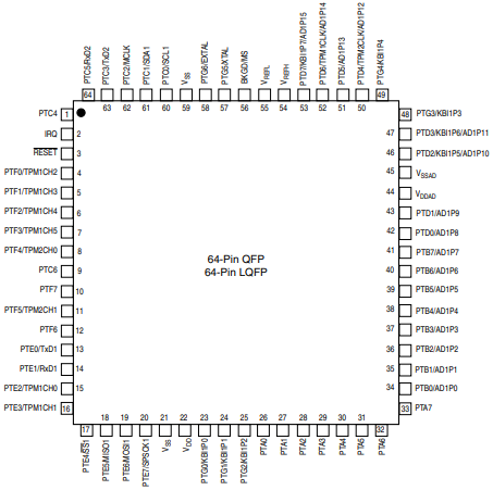
3. Pin configuration

4. Power supply
VDD and VSS are the main power supplies of the MCU. This voltage source is all power sources. I/O buffer circuit and internal regulator. Internal regulator provides voltage regulation Low voltage source for CPU and other internal circuits of MCU. Often, the application system has two independent reasons indirectly. In this case, there is Should be large-capacity research knowledge, such as 10-μF comprehensive, to provide large-capacity storage storage Used in the whole system and a 0.1μF ceramic ceramic, which is near VDD and VSS MC9S08AW6 has a second VSS sound. Correspondingly connected to the system ground plane or connected to the main VSS through low Contact information. VDD and VSSAD are the analog power supply of MCU. The voltage source is ADC module. Practical noise suppression.
5. Foldable
After reset, the MCU uses the internally generated clock (self-locking mode-fSelf_reset), which is equivalent to A speed of about 8 MHz is used as the speed. This frequency source is used at initial startup and can be The MCU also includes a stop-recovery light source, which requires a long start-up delay. The internal event (ICG) module that can be used to run the MCU can be fine-tuned. For ICG. These restrictions on XTAL are restricted by low attributes. For environmental weeds, the high gain output (HGO) bit can be set to Enable trace tracing. The accessory in this MCU is Pierce Hold, which can be formed or manufactured in-house. One of two frequency ranges selected by the RANGE bit in the ICGC1 electromagnetic. Ceramic, external can be connected to EXTAL input. RS (when used) and RF should be low inductance winding searchers and some metal composite searchers, there are C1 and C2 should usually be early childhood, dedicated to intimacy. Designed for high frequency applications. RF is used to provide a path to keep the EXTAL input within its linear range during startup, This value is usually not important. A typical system uses 1 MΩ to 10 MΩ. And the lower value will decrease and may not (in an emergency) be prevented from starting. C1 and C2 are usually in the range of 5-pF to 25-pF and are selected to meet specific requirements Must consider printed circuit board (PCB) capacitance and MCU circuit board Adjust the capacitance of C1 and C2. Crystal manufacturers usually specify a load capacitance It is usually a combination of C1 and C2 of the same size. Use 10 pF and each word (EXTAL 10XTAL).
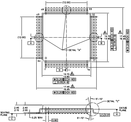
6. Package overview
