Can ship immediately
Due to market price fluctuations,if you need to purchase or consult the price.You can contact us or emial to us: brenda@hongda-ic.com
1. Description
The TI MSP family of ultra-low-power microcontrollers consists of several devices featuring different sets of peripherals targeted for various applications. The architecture, combined with extensive low-power modes, is optimized to achieve extended battery life in portable measurement applications. The device features a powerful 16-bit RISC CPU, 16-bit registers, and constant generators that contribute to maximum code efficiency. The digitally controlled oscillator (DCO) allows the device to wake up from low-power modes to active mode in 3.5 µs (typical).
2. Features
1. Low supply voltage range: 3.6 V down to 1.8 V
2. Ultra-low power consumption
– Active mode (AM): all system clocks active
- 230 µA/MHz at 8 MHz, 3.0 V, flash program execution (typical)
- 110 µA/MHz at 8 MHz, 3.0 V, RAM program execution (typical)
– Standby mode (LPM3): real-time clock (RTC) with crystal, watchdog, and supply supervisor operational, full RAM
- retention, fast wakeup: 1.7 µA at 2.2 V, 2.1 µA at 3.0 V (typical) low-power oscillator (VLO), general-purpose counter, watchdog, and supply supervisor
- operational, full RAM retention, fast wakeup: 1.2 µA at 3.0 V (typical)
– Off mode (LPM4): full RAM retention, supply supervisor
- operational, fast wakeup: 1.2 µA at 3.0 V (typical)
– Shutdown mode (LPM4.5): 0.1 µA at 3.0 V (typical)
3. Wake up from standby mode in 3.5 µs (typical)
4. 16-bit RISC architecture
– Extended memory
– Up to 25-MHz system clock
5. Flexible power-management system
– Fully integrated LDO with programmable regulated core supply voltage
– Supply voltage supervision, monitoring, and brownout
6. Unified clock system
– FLL control loop for frequency stabilization
– Low-power low-frequency internal clock source (VLO)
– Low-frequency trimmed internal reference source (REFO)
– 32-kHz crystals
– High-frequency crystals up to 32 MHz
7. 16-bit timer TA0, Timer_A with five capture/ compare registers
8. 16-bit timer TA1, Timer_A with three capture/ compare registers
9. 16-bit timer TB0, Timer_B with seven capture/ compare shadow registers
10. Up to four universal serial communication interfaces (USCIs)
– USCI_A0, USCI_A1, USCI_A2, and USCI_A3 each support:
11. Enhanced UART supports automatic baudrate detection
12. IrDA encoder and decoder
13. Synchronous SPI
– USCI_B0, USCI_B1, USCI_B2, and USCI_B3 each support:
14. I2C
15. Synchronous SPI
16. 12-bit analog-to-digital converter (ADC)
– Internal reference
– Sample-and-hold
– Autoscan feature
– 14 external channels, 2 internal channels
17. Hardware multiplier supports 32-bit operations
18. Serial onboard programming, no external programming voltage needed
19. 3-channel internal DMA
20. Basic timer with RTC feature
21. Device Comparison summarizes the available family members
3. Applications
1. Analog and Digital Sensor Systems
2. Digital Motor Controls
3. Remote Controls
4. Thermostats
5. Digital Timers
6. Hand-Held Meters
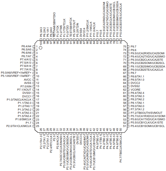
4. Pin configuration

5. Detailed Description
1. CPU
The MSP430 CPU has a 16-bit RISC architecture that is highly transparent to the application. All operations,other than program-flow instructions, are performed as register operations in conjunction with seven addressing modes for source operand and four addressing modes for destination operand. The CPU is integrated with 16 registers that provide reduced instruction execution time. The register-to-register operation execution time is one cycle of the CPU clock. Four of the registers, R0 to R3, are dedicated as program counter, stack pointer, status register, and constant generator, respectively. The remaining registers are general-purpose registers. Peripherals are connected to the CPU using data, address, and control buses. Peripherals can be managed with all instructions. The instruction set consists of the original 51 instructions with three formats and seven address modes and additional instructions for the expanded address range. Each instruction can operate on word and byte data.
2. Operating Modes
1. Active mode (AM)
– All clocks are active
2. Low-power mode 0 (LPM0)
– CPU is disabled
– ACLK and SMCLK remain active
– MCLK is disabled
– FLL loop control remains active
3. Low-power mode 1 (LPM1)
– CPU is disabled
– FLL loop control is disabled
– ACLK and SMCLK remain active
– MCLK is disabled
4. Low-power mode 2 (LPM2)
– CPU is disabled
– MCLK, FLL loop control, and DCOCLK are disabled
– DC generator of the DCO remains enabled
– ACLK remains active
5. Low-power mode 3 (LPM3)
– CPU is disabled
– MCLK, FLL loop control, and DCOCLK are disabled
– DC generator of the DCO is disabled
– ACLK remains active
6. Low-power mode 4 (LPM4)
– CPU is disabled
– ACLK is disabled
– MCLK, FLL loop control, and DCOCLK are disabled
– DC generator of the DCO is disabled
– Crystal oscillator is stopped
– Complete data retention
7. Low-power mode 4.5 (LPM4.5)
– Internal regulator disabled
– No data retention
– Wake-up input from RST or digital I/O