Can ship immediately
Due to market price fluctuations,if you need to purchase or consult the price.You can contact us or emial to us: brenda@hongda-ic.com
1. Describe
The PIC16F15313-E/RF microcontrollers feature analog, core-independent peripherals and communication peripherals, combined with Very Low Power (XLP) technology, for a wide range of general- purpose and low-power applications. These devices feature multiple PWMs, multiple communications, temperature sensors, and memory capabilities such as memory Access Partition (MAP) to support customer's data protection and bootloader applications and Device Information Area (DIA) where factory calibrated values are stored to help improve temperature sensor accuracy.
2. Feature
1. C compiler optimized RISC architecture
2. Running speed:
- DC – 32 MHz clock input
- 125 ns minimum instruction cycle
3. Interrupt capability
4. 16-level deep hardware stack
5. Timer:
- 8-bit Timer2 with Hardware Limit Timer (HLT)
- 16-bit timer 0/1
6. Low current power-on reset (POR)
7. Configurable Power-Up Timer (PWRTE)
8. Brown-out Reset (BOR)
9. Low Power BOR (LPBOR) option
10. Windowed Watchdog Timer (WWDT):
- Variable prescaler selection
- Variable window size selection
- All sources configured in hardware or software
11. Programmable code protection
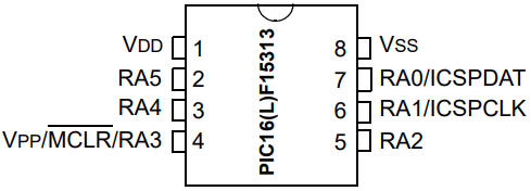
3. Pin configuration

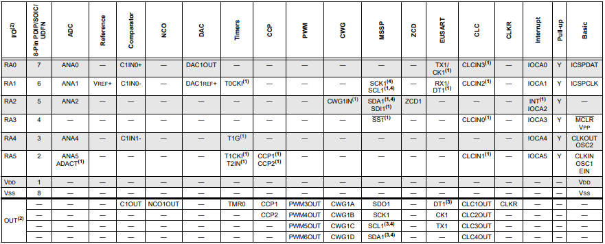
4. Pin Description

5. Power saving function
1. Doze Mode: Ability to run CPU cores more slowly than the system clock
2. Idle Mode: Ability to stop CPU cores internally Peripherals continue to operate
3. Sleep mode: lowest power consumption
4. Peripheral Module Disable (PMD):
- Ability to disable hardware modules Minimize active power consumption unused peripherals
6. Very Low Power (XLP) Features
1. Sleep Mode: 50 nA @ 1.8V, typical
2. Watchdog Timer: 500 nA @ 1.8V, typical
3. Working current:
- 8 μA @ 32 kHz, 1.8V, typical
- 32 μA/MHz @ 1.8V, typical
7. Digital peripherals
1. Four Configurable Logic Cells (CLCs):
- Integrated combinatorial and sequential logic
2. Complementary Waveform Generator (CWG):
- Rising and falling edge dead-band control
- Full-bridge, half-bridge, 1-channel driver
- Multiple signal sources
3. Two Capture/Compare/PWM (CCP) modules:
- 16-bit resolution in capture/compare mode
- 10-bit resolution in PWM mode
4. Four 10-bit PWMs
5. Numerically Controlled Oscillator (NCO):
- yields true linear frequency control and Improve frequency resolution
- Input Clock: 0 Hz < FNCO < 32 MHz
- Resolution: FNCO/220
6. One EUSART, RS-232, RS-485, LIN compatible
7. I/O pins:
- Individually programmable pull-ups
- Slew rate control
- Change interrupt with edge selection
- Input level selection control (ST or TTL)
- Digital open-drain enable
8. Peripheral Pin Select (PPS):
- Enable pin mapping of digital I/O
8. Analog peripherals
1. Analog-to-Digital Converter (ADC):
- 10 bits, up to 43 external channels
- run in sleep
2. Up to two comparators:
- FVR, DAC and external input pins available for inverting and non-inverting inputs
- Software selectable hysteresis
- Outputs can be provided internally to other modules or externally via PPS
3. 5 digital-to-analog converters (DACs):
- 5-bit resolution, rail-to-rail
- Positive reference selection
- Unbuffered I/O pin output
- Internal connection to ADC and comparator
4. Reference voltage:
- Fixed voltage reference with 1.024V, 2.048V and 4.096V output levels
5. Zero-Crossing Detection Module:
- AC high voltage zero-crossing detection for simplified TRIAC control
- Synchronized switch control and timing
9. Flexible oscillator structure
1. High Precision Internal Oscillator:
- Software selectable frequency range up to 32 MHz, typical ±1%
2. x2/x4 PLL with internal and external sources
3. Low power internal 31 kHz oscillator (LFINTOSC)
4. External oscillator block:
- Three crystal/resonator modes up to 20 MHz
- Three external clock modes up to 32 MHz
5. Failsafe Clock Monitor:
- Allows safe shutdown if master clock is stopped
6. Oscillator Start-up Timer (OST):
- Ensure the stability of crystal oscillator resources