Can ship immediately
Due to market price fluctuations,if you need to purchase or consult the price.You can contact us or emial to us: brenda@hongda-ic.com
1. Describe
TLC272CDR and TLC277 precision dual Operational amplifiers combine a wide range of Input offset voltage level with low offset voltage Drift, high input impedance, low noise and speed Close to those general-purpose BiFET devices. These devices use Texas Instruments’ silicongate LinCMOS® technology, which provides Offset voltage stability far exceeds stability It can be used in traditional metal gate process. Very high input impedance, low bias The current and high conversion rate make these cost-effective devices ideal for previous applications Reserved for BiFET and NFET products. Four Provide bias voltage level (C suffix and I-suffix type), ranging from low-cost TLC272 (10 mV) to high precision TLC277 (500 µV). Generally speaking, LinCMOStm operational amplifiers have many functions related to bipolar technology There is no power loss of bipolar technology. General applications, such as sensor interface, analog Calculations, amplifier modules, active filters and signal buffers can use TLC272 and TLC277. These devices also exhibit low-voltage single-supply operation, making them ideal for remote And inaccessible battery-powered apps. Common mode input voltage range includes negative rail. A variety of packaging options are available, including small form factor and chip carrier versions for high density system applications. The device inputs and outputs are designed to withstand –100mA surge current without continuous latch-up. TLC272 and TLC277 contain internal ESD protection circuits, which can prevent functional failures under voltage. Tested according to MIL-STD-883C, Method 3015.2, up to 2000 V; however, care should be taken when handling these devices when exposed to ESD which may lead to device parameter performance decline. The feature of the C suffix device is that it can work in a temperature range of 0°C to 70°C. The characteristics of I-suffix devices are suitable for operation from –40°C to 85°C. M-suffix equipment is characterized by operating in a temperature range of –55°C to 125°C throughout the military range.
2. Feature
1. Trimmed Offset Voltage: TLC277 . . . 500 µV Max at 25°C, VDD = 5 V
2. Input Offset Voltage Drift ...Typically 0.1 µV/Month, Including the First 30 Days
3. Wide Range of Supply Voltages Over Specified Temperature Range:
– 0°C to 70°C . . . 3 V to 16 V
– 40°C to 85°C . . . 4 V to 16 V
– 55°C to 125°C . . . 4 V to 16 V
4. Single-Supply Operation
5. Common-Mode Input Voltage Range Extends Below the Negative Rail (C-Suffix, I-Suffix types)
6. Low Noise ...Typically 25 nV/√Hz at f = 1 kHz
7. Output Voltage Range Includes Negative Rail
8. High Input impedance . . . 1012 Ω Typ
9. ESD-Protection Circuitry
10. Small-Outline Package Option Also Available in Tape and Reel
11. Designed-In Latch-Up Immunity
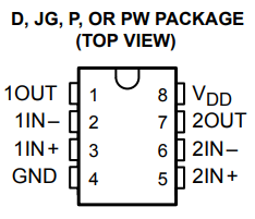
3. Pin configuration
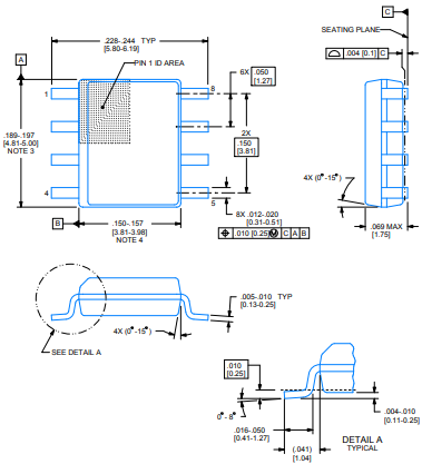
4. Package overview