Can ship immediately
Due to market price fluctuations,if you need to purchase or consult the price.You can contact us or emial to us: brenda@hongda-ic.com
1. Describe
STM8S003F3P6 Value Line 8-bit microcontrollers with 8 KB Flash program memory and integrated real data EEPROM. The STM8S003F3/K3 Value Line devices offer the following advantages: performance, robustness and reduced system cost. True data EEPROM supporting up to 100,000 write/erase cycles, state-of-the-art core and peripherals built with 16 MHz clock frequency, powerful I/Os, independent watchdogs, and independent clock sources and clock security system. Reduced system cost due to high system integration with internal clock oscillator, watchdog and brown-out reset.
2. Features
1. Core
- 16 MHz advanced STM8 core with Harvard architecture and 3-stage pipeline
- Extended instruction set
2. Memories
- Program memory: 8 Kbyte Flash memory; data retention 20 years at 55 °C after 100 cycles
- RAM: 1 Kbyte
- Data memory: 128 bytes true data EEPROM; endurance up to 100 k write/erase cycles
3. Clock, reset and supply management
1. 2.95 V to 5.5 V operating voltage
2. Flexible clock control, 4 master clock sources
– Low-power crystal resonator oscillator
– External clock input
– Internal, user-trimmable 16 MHz RC
– Internal low-power 128 kHz RC
3. Clock security system with clock monitor
4. Power management
– Low-power modes (wait, active-halt, halt)
– Switch-off peripheral clocks individually
– Permanently active, low-consumption power-on and power-down reset
4. Interrupt management
- Nested interrupt controller with 32 interrupts
- Up to 27 external interrupts on 6 vectors
5. Timers
- Advanced control timer: 16-bit, 4 CAPCOM channels, 3 complementary outputs, dead-time insertion and flexible synchronization
- 16-bit general purpose timer, with 3 CAPCOM channels (IC, OC or PWM)
- 8-bit basic timer with 8-bit prescaler
- Auto wakeup timer
- Window and independent watchdog timers
6. Communications interfaces
- UART with clock output for synchronous operation, SmartCard, IrDA, LIN master mode
- SPI interface up to 8 Mbit/s
- I2C interface up to 400 Kbit/s
7. Analog to digital converter (ADC)
- 10-bit ADC, ± 1 LSB ADC with up to 5 multiplexed channels, scan mode and analog watchdog
8. I/Os
- Up to 28 I/Os on a 32-pin package including 21 high-sink outputs
- Highly robust I/O design, immune against current injection
9. Development support
- Embedded single-wire interface module (SWIM) for fast on-chip programming and nonintrusive debugging
3. Analog-to-digital converter (ADC1)
1. Input voltage range: 0 to VDDA
2. Conversion time: 14 clock cycles
3. Single and continuous, buffered continuous conversion modes
4. Buffer size (10 x 10 bits)
5. Scan mode for single and continuous conversion of a sequence of channels
6. Analog watchdog capability with programmable upper and lower thresholds
7. Analog watchdog interrupt
8. External trigger input
9. Trigger from TIM1 TRGO
10. End of conversion (EOC) interrupt
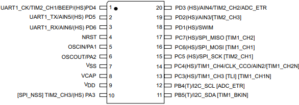
4. Pin configuration
