Can ship immediately
Due to market price fluctuations,if you need to purchase or consult the price.You can contact us or emial to us: brenda@hongda-ic.com
1. Description
The STM8S903K3T6C access line 8-bit microcontrollers offer 8 Kbyte Flash program memory, plus integrated true data EEPROM.benefits: performance, robustness, and reduced system cost.Device performance and robustness are ensured by advanced core and peripherals made in a state-of-the art technology, a 16 MHz clock frequency, robust I/Os, independent watchdogs with separate clock source, and a clock security system. The system cost is reduced thanks to an integrated true data EEPROM for up to 300 k write/erase cycles and a high system integration level with internal clock oscillators, watchdog and brown-out reset. Full documentation is offered as well as a wide choice of development tools.
2. Features
1. Core
1. 16 MHz advanced STM8 core with Harvard architecture and 3-stage pipeline
2. Extended instruction set
2. Memories
1. Program memory: 8 Kbyte Flash; data retention 20 years at 55 °C after 10 kcycle
2. Data memory: 640 byte true data EEPROM; endurance 300 kcycle
3. RAM: 1 Kbyte
3. Clock, reset and supply management
1. 2.95 to 5.5 V operating voltage
2. Flexible clock control, 4 master clock sources
– Low power crystal resonator oscillator
– External clock input
– Internal, user-trimmable 16 MHz RC
– Internal low-power 128 kHz RC
3. Clock security system with clock monitor
4. Power management:
– Low-power modes (wait, active-halt, halt)
– Switch-off peripheral clocks individually
5. Permanently active, low-consumption poweron and power-down reset
4. Interrupt management
1. Nested interrupt controller with 32 interrupts
2. Up to 28 external interrupts on 7 vectors
5. Timers
1. Advanced control timer: 16-bit, 4 CAPCOM channels, 3 complementary outputs, dead-time insertion and flexible synchronization
2. 16-bit general purpose timer, with 3 CAPCOM channels (IC, OC or PWM)
3. 8-bit basic timer with 8-bit prescaler
4. Auto wake-up timer
5. Window watchdog and independent watchdog timers
6. Communication interfaces
1. UART with clock output for synchronous operation, SmartCard, IrDA, LIN master mode
2. SPI interface up to 8 Mbit/s
3. I2C interface up to 400 kbit/s
7. Analog to digital converter (ADC)
1. 10-bit, ±1 LSB ADC with up to 7 multiplexed channels + 1 internal channel, scan mode and analog watchdog
2. Internal reference voltage measurement
8. I/Os
1. Up to 28 I/Os on a 32-pin package including 21 high sink outputs
2. Highly robust I/O design, immune against current injection
9. Unique ID
1. 96-bit unique key for each device
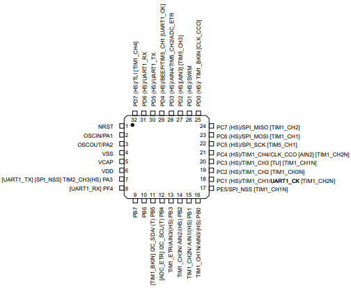
3. STM8S903K3 pinout

4. Minimum and maximum values
Unless otherwise specified the minimum and maximum values are guaranteed in the worst conditions of ambient temperature, supply voltage and frequencies by tests in production on 100% of the devices with an ambient temperature at TA = 25 °C, and TA = TAmax (given by the selected temperature range). Data based on characterization results, design simulation and/or technology characteristics are indicated in the table footnotes and are not tested in production. Based on characterization, the minimum and maximum values refer to sample tests and represent the mean value plus or minus three times the standard deviation (mean ± 3 Σ).
5. Typical values
Unless otherwise specified, typical data are based on TA = 25 °C, VDD = 5.0 V. They are given only as design guidelines and are not tested. Typical ADC accuracy values are determined by characterization of a batch of samples from a standard diffusion lot over the full temperature range, where 95% of the devices have an error less than or equal to the value indicated (mean ± 2 Σ).
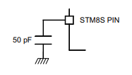
6. Load capacitance
Load conditions for pin parameter measurement
