Can ship immediately
1. Description
This two-bit non-inverting translator is a bidirectional voltage-level translator and can be used to establish digital switching compatibility between mixed-voltage systems. It uses two separate configurable powersupply rails, with the A ports supporting operating voltages from 1.65 V to 3.6 V while it tracks the VCCA supply, and the B ports supporting operating voltages from 2.3 V to 5.5 V while it tracks the VCCB supply. This allows the support of both lower and higher logic signal levels while providing bidirectional translation capabilities between any of the 1.8-V, 2.5-V, 3.3-V, and 5-V voltage nodes.
When the output-enable (OE) input is low, all I/Os are placed in the high-impedance state, which significantly reduces the power-supply quiescent current consumption. To ensure the high-impedance state during power up or power down, OE should be tied to GND through a pulldown resistor; the minimum value of the resistor is determined by the current-sourcing capability of the driver.
2. Features
1. No Direction-Control Signal Needed
2. Maximum Data Rates
– 24 Mbps (Push Pull)
– 2 Mbps (Open Drain)
3. Available in the Texas Instruments NanoStar™ Package
4. 1.65 V to 3.6 V on A Port and 2.3 V to 5.5 V on B Port (VCCA ≤ VCCB)
5. VCC Isolation Feature: If Either VCC Input Is at GND, Both Ports Are in the High-Impedance State
6. No Power-Supply Sequencing Required: Either VCCA or VCCB Can Be Ramped First
7. Ioff Supports Partial-Power-Down Mode Operation
8. Latch-Up Performance Exceeds 100 mA Per JESD 78, Class II
9. ESD Protection Exceeds JESD 22
– A Port:
2500-V Human-Body Model (A114-B)
250-V Machine Model (A115-A)
1500-V Charged-Device Model (C101)
– B Port:
8-kV Human-Body Model (A114-B)
250-V Machine Model (A115-A)
1500-V Charged-Device Model (C101)
3. Applications
1. I2C / SMBus
2. UART
3. GPIO
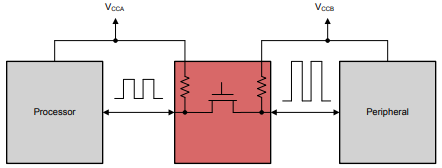
4. Typical Application Block Diagram for TXS0102DCUR

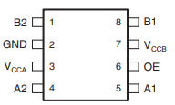
5. Pin Configuration and Functions

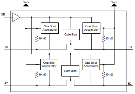
6. Functional Block Diagram
